


 Punching Out: Breaking Out of the Valuation Box
 Happy’s Tech Talk #28: The Power Mesh Architecture for PCBs
 It’s Only Common Sense: Would You Join Your Own Company?
Mysterious Quantum Properties in Material Point to New Applications in Electronics
September 26, 2016 | Lawrence Berkeley National LaboratoryEstimated reading time: 5 minutes
Researchers have created an exotic 3-D racetrack for electrons in ultrathin slices of a nanomaterial they fabricated at the Department of Energy’s Lawrence Berkeley National Laboratory (Berkeley Lab).
The international team of scientists from Berkeley Lab, UC Berkeley, and Germany observed, for the first time, a unique behavior in which electrons rotate around one surface, then through the bulk of the material to its opposite surface and back.
The possibility of developing so-called “topological matter” that can carry electrical current on its surface without loss at room temperature has attracted significant interest in the research community. The ultimate goal is to approach the lossless conduction of another class of materials, known as superconductors, but without the need for the extreme, freezing temperatures that superconductors require.
“Microchips lose so much energy through heat dissipation that it’s a limiting factor,” said James Analytis, a staff scientist at Berkeley Lab and assistant professor of physics at UC Berkeley who led the study, published in Nature. “The smaller they become, the more they heat up.”
The studied material, an inorganic semimetal called cadmium arsenide (Cd3As2), exhibits quantum properties—which are not explained by the classical laws of physics—that offer a new approach to reducing waste energy in microchips. In 2014, scientists discovered that cadmium arsenide shares some electronic properties with graphene, a single-atom-thick material also eyed for next-generation computer components, but in a 3-D form.
“What’s exciting about these phenomena is that, in theory, they are not affected by temperature, and the fact they exist in three dimensions possibly makes fabrication of new devices easier,” Analytis said.
The cadmium arsenide samples displayed a quantum property known as “chirality” that couples an electron’s fundamental property of spin to its momentum, essentially giving it left- or right-handed traits. The experiment provided a first step toward the goal of using chirality for transporting charge and energy through a material without loss.
In the experiment, researchers manufactured and studied how electric current travels in slices of a cadmium arsenic crystal just 150 nanometers thick, or about 600 times smaller than the width of a human hair, when subjected to a high magnetic field.
The crystal samples were crafted at Berkeley Lab’s Molecular Foundry, which has a focus in building and studying nanoscale materials, and their 3-D structure was detailed using X-rays at Berkeley Lab’s Advanced Light Source.
Many mysteries remain about the exotic properties of the studied material, and as a next step researchers are seeking other fabrication techniques to build a similar material with built-in magnetic properties, so no external magnetic field is required.
“This isn’t the right material for an application, but it tells us we’re on the right track,” Analytis said.
If researchers are successful in their modifications, such a material could conceivably be used for constructing interconnects between multiple computer chips, for example, for next-generation computers that rely on an electron’s spin to process data (known as “spintronics”), and for building thermoelectric devices that convert waste heat to electric current.
It wasn’t clear at first whether the research team would even be able to manufacture a pure enough sample at the tiny scale required to carry out the experiment, Analytis said.
“We wanted to measure the surface states of electrons in the material. But this 3-D material also conducts electricity in the bulk—it’s central region—as well as at the surface,” he said. As a result, when you measure the electric current, the signal is swamped by what is going on in the bulk so you never see the surface contribution.”
So they shrunk the sample from millionths of a meter to the nanoscale to give them more surface area and ensure that the surface signal would be the dominant one in an experiment.
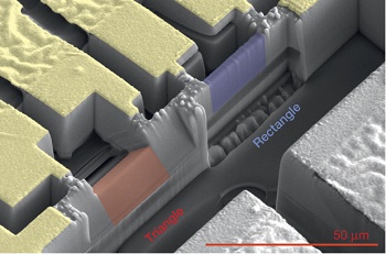
This image, produced by a scanning electron microscope, shows three sheets of a crystal material called cadmium arsenide. The finely polished rectangular sheets (purple) were sliced from the same crystal in varying thicknesses. They measure about 4 microns (thousandths of a millimeter) tall by 10 microns wide.
Page 1 of 2
Share on:


Suggested Items
Ansys’ Collaboration with Schrödinger will Accelerate Materials Development with Unprecedented Multiscale Simulation
05/09/2024 | ANSYSAnsys and Schrödinger are collaborating to deliver an ICME approach that bridges the gap between materials discovery and product development.
2024 Apple iPad Pro Estimated to Ship Between 4.5 to 5 Million Units
05/08/2024 | TrendForceApple’s recent product launch in May introduced a lineup of new tablets featuring advanced AMOLED screens. Notably, the Pro version boasts a dual-layer tandem structure designed to address the longstanding challenges of screen burn-in and lifespan that are common with AMOLED displays.
AIM Solder Signs Shinil Fl Ltd. as New Distributor for Korea
05/08/2024 | AIM SolderAIM Solder, a leading global manufacturer of solder assembly materials for the electronics industry, is pleased to announce a new distribution partnership with Shinil Fl Ltd., a prominent supplier of technological solutions in the SMT and semiconductor sectors.
IDTechEx Discusses Low-Loss Materials: The Enabler of Future Connected Vehicles?
05/06/2024 | IDTechExFuture connected vehicles will offer future drivers a safer, smoother, and more convenient driving experience. Not only will drivers get access to more navigation and entertainment options, but they will also gain access to safety technologies that will potentially reduce accidents, improve congestion, and reduce emissions globally by allowing vehicle safety systems to communicate with each other and with city traffic infrastructure.
LQDX Divests Aluminum Soldering Business - Mina™ - to Taiyo America Inc.
05/02/2024 | PRNewswireLQDX, formerly known as Averatek Corp., developer of high-performance materials for advanced semiconductor manufacturing, today announced that it has divested its aluminum soldering business – known as MinaTM – to Taiyo America Inc., a global market leader in advanced electronic materials.