


 The Chemical Connection: Reducing Etch System Water Usage, Part 2
 It’s Only Common Sense: Nice Guys Really Can Finish First
 The Right Approach: I Hear the Train A Comin'
Two-Dimensional MXene Materials Get Their Close-Up
March 16, 2017 | ORNLEstimated reading time: 4 minutes
Researchers have long sought electrically conductive materials for economical energy-storage devices. Two-dimensional (2D) ceramics called MXenes are contenders. Unlike most 2D ceramics, MXenes have inherently good conductivity because they are molecular sheets made from the carbides and nitrides of transition metals like titanium.
MXenes were co-discovered by Michael Naguib, now a Wigner Fellow at the Department of Energy’s Oak Ridge National Laboratory, while pursuing his PhD at Drexel University in 2011. MXene layers can be combined to engineer ultrathin electronics, sensors, batteries, supercapacitors and catalysts. About 20 MXenes have since been reported.
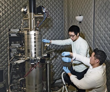
Recently, ORNL scientists using state-of-the-art scanning transmission electron microscopy, or STEM, provided the first direct evidence of the atomic-defect configurations in a titanium-carbide MXene synthesized at Drexel University. Published in ACS Nano, a journal of the American Chemical Society, the study coupled atomic-scale characterization and electrical property measurements with theory-based simulation.
“Using atomic-resolution scanning transmission electron microscopy imaging, we visualized defects and defects clusters in MXene that are very important for future nano electronic devices and catalytic applications,” said lead author Xiahan Sang of the Center for Nanophase Materials Sciences (CNMS), a DOE Office of Science User Facility at ORNL.
“Atomic-level defects can be engineered into materials to enable new functionalities,” said senior author Raymond Unocic of CNMS. “Understanding these defects is critical for advancing materials.”
Atomic imaging from different perspectives was the key to revealing MXene’s structure. When the sample is aligned with the electron beam within a STEM instrument, the viewer cannot tell how many sheets lie under the top layer. But simply tilt the sample, and differences readily appear. For example, a multi-sheet layer is made of stacked atoms, a structure that forms a blurred image when the layer is tilted. The appearance of sharp atomic images under different tilting conditions unambiguously proved the single-layer structure of the MXene.
Easy mass-production of a good 2D conductor
MXenes are made from a three-dimensional (3D) bulk crystal called MAX (the “M” denotes a transition metal; “A,” an element, such as aluminum or silicon, from a specific chemical group; and “X,” either carbon or nitrogen). In the MAX lattice from which the MXene explored in this study emerged, three layers of titanium carbide are sandwiched between aluminum layers.
The Drexel researchers improved a technique developed in 2011 and altered in 2014 to synthesize MXene from the bulk MAX phase using acids. The improved method is called minimally intensive layer delamination, or MILD. “By going with MILD, we ended up with large flakes of high-quality MXene,” said Mohamed Alhabeb, a PhD student in materials science at Drexel University, who accomplished this feat with another PhD student, Katherine Van Aken, under the leadership of one of the co-discoverers of MXenes, Distinguished University Professor and Director of the A.J. Drexel Nanomaterials Institute Yury Gogotsi.
To synthesize free-standing MXene flakes, the Drexel team first treated bulk MAX with an etchant of fluoride salt and hydrochloric acid to selectively remove unwanted layers of aluminum from between titanium carbide layers. Then they manually shook the etched material to separate and collect the titanium carbide layers. Each layer is five atoms thick and is made of carbon atoms binding three titanium sheets. Etching and exfoliating MAX produces many of these free-standing MXene layers. This relatively simple technique may enable manufacturing-scale production.
Etching creates defects—vacant spaces that emerge as titanium atoms are pulled from surfaces. “Defects” are actually good in many applications of materials. They can be introduced into a material and manipulated to enhance its useful catalytic, optical or electronic properties.
The greater the concentration of etchant, the larger the number of defects created, the study found. “We have the capability to tune the defect concentration, which could be used to tailor physicochemical properties for energy storage and conversion devices,” Sang said.
Moreover, the number of defects did not strongly affect MXene’s electrical conductivity. At CNMS, Ming-Wei Lin and Kai Xiao measured physical properties, including electrical conductivity, of various promising 2D materials. They found MXene was an order of magnitude less conductive than a perfect graphene sheet but two orders of magnitude more conductive than metallic molybdenum disulfide.
Using modeling and simulation, ORNL’s Paul Kent and Yu Xie calculated the energy needed to create atomic configurations of defects that Sang’s STEM showed were prevalent.
Next the researchers plan to tune defects down to the atomic level to tailor specific behaviors.
The title of the paper is “Atomic Defects in Monolayer Titanium Carbide (Ti3C2Tx) MXene.”
The Fluid Interface Reactions, Structures and Transport (FIRST) Center, an Energy Frontier Research Center led by ORNL and funded by DOE’s Office of Science, supported the study. FIRST aims to develop scientific understanding and validated, predictive models of the nanoscale environment at fluid–solid interfaces important in electrical energy storage and electrocatalysis.
Aberration-corrected STEM imaging and device fabrication and measurements were conducted at CNMS, a DOE Office of Science User Facility at ORNL. The research also used resources of the National Energy Research Scientific Computing Center, a DOE Office of Science User Facility at Lawrence Berkeley National Laboratory.
Share on:


Suggested Items
LQDX Divests Aluminum Soldering Business - Mina™ - to Taiyo America Inc.
05/02/2024 | PRNewswireLQDX, formerly known as Averatek Corp., developer of high-performance materials for advanced semiconductor manufacturing, today announced that it has divested its aluminum soldering business – known as MinaTM – to Taiyo America Inc., a global market leader in advanced electronic materials.
Indium Corporation Expert to Present on Pb-Free Solder for Die-Attach in Discrete Power Applications
04/30/2024 | Indium CorporationIndium Corporation Product Manager – Semiconductor Dean Payne will present at the Advanced Packaging for Power Electronics conference, hosted by IMAPS, held May 8-9 in Woburn, Massachusetts, USA.
Real Time with... IPC APEX EXPO 2024: Adhesive Materials and Equipment Update with Dymax
05/01/2024 | Real Time with...IPC APEX EXPOVirginia Hogan, global business development manager at Dymax, discusses adhesive materials, dispensing and curing equipment, a new, high-reliability conformal coating, and various materials and dispensing methods.
Real Time with... IPC APEX EXPO 2024: Sustainability in the Industry
04/26/2024 | Real Time with...IPC APEX EXPOGuest Editor Henry Crandall and Chris Nash of Indium Corporation discuss the company's 90th anniversary and its focus on sustainability. They focus on the benefits of sustainable materials, their compatibility, and value propositions. The conversation also highlights how Durafuse LT technology's role in reducing reflow temperatures is leading to significant cost and energy savings. Nash also touches on downstream sustainability efforts such as using recycled materials for packaging.
SMC Korea 2024 to Highlight Semiconductor Materials Trends and Innovations on Industry’s Path to $1 Trillion
04/24/2024 | SEMIWith Korea a major consumer of semiconductor materials and advanced materials a key driver of innovation on the industry’s path to $1 trillion, industry leaders and experts will gather at SMC (Strategic Materials Conference) Korea 2024 on May 29 at the Suwon Convention Center in Gyeonggi-do, South Korea to provide insights into the latest materials developments and trends. Registration is open.