


 It’s Only Common Sense: Nice Guys Really Can Finish First
 The Right Approach: I Hear the Train A Comin'
 Marcy's Musings: The Growing Industry
Aven's New Wide-View UV Magnifier with White & Ultraviolet LEDs
January 31, 2023 | AvenEstimated reading time: Less than a minute
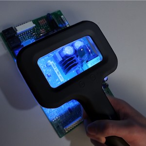
Aven, a full-service technology provider, is pleased to introduce its Wide-View Magnifier [2.25x | 4x] with Ultraviolet and White LEDs. Convenient and easy-to-use, Aven’s Wide-View UV Magnifier features a 3.6 x 1.7” rectangular glass, providing a wide viewing area. The 5-diopter lens offers up to 2.25X magnification, and the 1” diameter spot lens increases the magnification to 4X.
Operating at 365 ?m, the UV LEDs are exceptionally bright when illuminating objects that fluoresce, such as paper, ink, circuit boards, money, etc. The 26 UV LEDs shine brightly to reveal fluoresced details that standard lights cannot show.
The Wide-View Magnifier is ideal for dermatology, trauma, schools, ophthalmology, forensic science, hospitality/food industry, agriculture, and industrial inspection for detecting defects. The ESD-safe design helps to dissipate static electric charges, protecting sensitive components below from unintentional damage.
As a result of years of comprehensive research and development, Aven has expanded its expertise in the realm of design and customized configuration of advanced video inspection systems. The company’s solution-based experts possess the ability to recommend and create complete optical systems according to customers’ needs and budgets.
Share on:


Suggested Items
Real Time with… IPC APEX EXPO 2024: Ventec Discusses New Pro-bond Family of Advanced Products
05/01/2024 | Real Time with...IPC APEX EXPOChris Hanson, Ventec's Global Head of IMS Technology, outlines the launch of four pro-bond formulas that deliver an outstanding combination of low dissipation factor (Df) with a dielectric constant (Dk) range to maximize the design window for critical PCB parameters. As Chris points out, Pro-bond is designed for low-loss, high-speed applications, while thermal-bond dissipates heat from a component through the board to a heat sink.
IPC's Vision for Empowering PCB Design Engineers
04/30/2024 | Robert Erickson, IPCAs architects of innovation, printed circuit board designers are tasked with translating increasingly complex concepts into tangible designs that power our modern world. IPC provides the necessary community, standards framework, and education to prepare these pioneers as they explore the boundaries of what’s possible, equipping engineers with the knowledge, skills, and resources required to thrive in an increasingly dynamic field.
iNEMI Packaging Tech Topic Series: Role of EDA in Advanced Semiconductor Packaging
04/26/2024 | iNEMIAdvanced semiconductor packaging with heterogenous integration has made on-package integration of multiple chips a crucial part of finding alternatives to transistor scaling. Historically, EDA tools for front-end and back-end design have evolved separately; however, design complexity and the increased number of die-to-die or die-to-substrate interconnections has led to the need for EDA tools that can support integration of overall design planning, implementation, and system analysis in a single cockpit.
Cadence, TSMC Collaborate on Wide-Ranging Innovations to Transform System and Semiconductor Design
04/25/2024 | Cadence Design SystemsCadence Design Systems, Inc. and TSMC have extended their longstanding collaboration by announcing a broad range of innovative technology advancements to accelerate design, including developments ranging from 3D-IC and advanced process nodes to design IP and photonics.
Ansys, TSMC Enable a Multiphysics Platform for Optics and Photonics, Addressing Needs of AI, HPC Silicon Systems
04/25/2024 | PRNewswireAnsys announced a collaboration with TSMC on multiphysics software for TSMC's Compact Universal Photonic Engines (COUPE). COUPE is a cutting-edge Silicon Photonics (SiPh) integration system and Co-Packaged Optics platform that mitigates coupling loss while significantly accelerating chip-to-chip and machine-to-machine communication.