


 It’s Only Common Sense: Nice Guys Really Can Finish First
 The Right Approach: I Hear the Train A Comin'
 Marcy's Musings: The Growing Industry
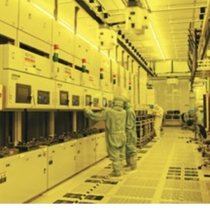
Fujitsu Develops Field Engineering Technology to Rapidly Provide IoT Services
May 25, 2016 | ACN NewswireEstimated reading time: 4 minutes
1. Radio wave simulation technology that can simply and automatically determine installation points for wireless devices
Fujitsu Laboratories has simplified the handling of radio wave simulations, which previously required huge amounts of time and effort, with the following two technologies, which can simply and automatically determine installation points for wireless devices, even without wireless device expertise.
1) 3D spatial digitizing technology:
Fujitsu Laboratories has developed technology to automatically create the 3D layout data necessary for radio wave simulations just by measuring with a laser scan from a few points around the site, and then automatically correcting distortions and smoothly merging measurement data from multiple scans. With this technology, the time required to create the layout data is shortened from around one week when creating it by hand to around two hours, including measurement time.
2) Moving body modeling technology:
In order to reflect the impact of people's movements numerically, it was previously necessary to run many simulations, changing the placement of people a bit each time. Now, by automatically measuring the number of people coming and going using technology developed by Fujitsu Laboratories that recognizes the flow of people from video(1), making patterns for different numbers of people, and using these in simulations, simulations that might have taken three days can now be done on an ordinary PC in less than fifteen minutes.
Figure 2: Radio wave simulation technology
2. Radio wave interference visualization technology
Fujitsu Laboratories has developed technology that automatically recognizes and displays wireless communications actually being used at sites where IoT devices are installed, and visualizes the state of signal congestion for each channel and location, and for each communications standard. This makes it possible, even for non-experts, to determine appropriate installation locations for IoT devices, data transmission time spacing, and channel settings.
This technology recognizes wireless standards (such as Wi-Fi, Bluetooth and ZigBee) through a unique computation method of correlation coefficient between received signals and signal patterns prepared for each wireless standard. Previous technology would perform a product-sum operation with signal patterns prepared for each standard, after frequency correction of the received signal, but this technology uses the fact that, when the received signal differs from the prepared signal pattern, the results of multiplication of the signal before frequency correction have high randomness to achieve high recognition performance, successfully improving recognition sensitivity to twice that of previous methods.
Figure 3: Radio wave interference visualization technology
Effects
With this newly developed technology, Fujitsu Laboratories has reduced the time required to install IoT devices at a site to one-third that of previous methods.
This means that, because the installation of wireless devices, which created issues for implementing and operating an IoT system, and radio wave congestion and interference countermeasures have become easier to do, when using an IoT system with the goal of achieving operational efficiencies or to create value, customers can greatly reduce the time needed before they start actual operations. In addition, even after starting operations, these technologies also make it possible to operate stably, without any major trouble causing operations to stop.
Page 2 of 2Share on:


Suggested Items
IDTechEx Report on Quantum Technology: Nano-scale Physics for Massive Market Impact
04/30/2024 | PRNewswireThe quantum technology market leverages nano-scale physics to create revolutionary new devices for computing, sensing, and communications. Across the industry, quantum technology offers a paradigm shift in performance compared with incumbent solutions.
TSMC Certifies Ansys Multiphysics Platforms, Enabling Next-Gen AI and HPC Chips
04/30/2024 | PRNewswireAnsys announced the certification of its power integrity platforms for TSMC's N2 technology full production release. Both Ansys RedHawk-SC and Ansys Totem are certified for power integrity signoff on the N2 process, delivering significant speed and power advantages for high performance computing, mobile chips, and 3D-IC designs.
Koh Young Extends Invitation to the 2024 IEEE Electronic Components and Technology Conference
04/30/2024 | Koh YoungKoh Young, the industry leader in True3D measurement-based inspection solutions, invites you to join us at the at the 2024 IEEE Electronic Components and Technology Conference from May 28-31, 2024, in Denver, Colorado at the Gaylord Rockies Resort & Convention Center.
Samsung Electronics Begins Industry’s First Mass Production of 9th-Gen V-NAND
04/29/2024 | Samsung ElectronicsSamsung Electronics, the world leader in advanced memory technology, today announced that it has begun mass production for its one-terabit (Tb) triple-level cell (TLC) 9th-generation vertical NAND (V-NAND), solidifying its leadership in the NAND flash market.
TSMC Celebrates 30th North America Technology Symposium
04/29/2024 | TSMCTSMC unveiled its newest semiconductor process, advanced packaging, and 3D IC technologies for powering the next generation of AI innovations with silicon leadership at the Company’s 2024 North America Technology Symposium.