


 The Right Approach: I Hear the Train A Comin'
 It’s Only Common Sense: OCCAM—the Time Is Now
 Marcy's Musings: The Growing Industry
Under Pressure: New Technique Could Make Large, Flexible Solar Panels More Feasible
May 17, 2016 | Pennsylvania State UniversityEstimated reading time: 1 minute
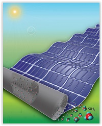
A new, high-pressure technique may allow the production of huge sheets of thin-film silicon semiconductors at low temperatures in simple reactors at a fraction of the size and cost of current technology. A paper describing the research by scientists at Penn State University publishes on May 13, 2016, in the journal Advanced Materials.
"We have developed a new, high-pressure, plasma-free approach to creating large-area, thin-film semiconductors," said John Badding, professor of chemistry, physics, and materials science and engineering at Penn State and the leader of the research team. "By putting the process under high pressure, our new technique could make it less expensive and easier to create the large, flexible semiconductors that are used in flat-panel monitors and solar cells and are the second most commercially important semiconductors."
Thin-film silicon semiconductors typically are made by the process of chemical vapor deposition, in which silane -- a gas composed of silicon and hydrogen -- undergoes a chemical reaction to deposit the silicon and hydrogen atoms in a thin layer to coat a surface. To create a functioning semiconductor, the chemical reaction that deposits the silicon onto the surface must happen at a low enough temperature so that the hydrogen atoms are incorporated into the coating rather than being driven off like steam from boiling water. With current technology, this low temperature is achieved by creating plasma -- a state of matter similar to a gas made up of ions and free electrons -- in a large volume of gas at low pressure. Massive and expensive reactors so large that they are difficult to ship by air are needed to generate the plasma and to accommodate the large volume of gas required.
"With our new high-pressure chemistry technique, we can create low-temperature reactions in much smaller spaces and with a much smaller volume of gas," said Badding. "The reduced space necessary allows us, for the first time, to create semiconductors on multiple, stacked surfaces simultaneously, rather than on just a single surface. To maximize the surface area, rolled-up flexible surfaces can be used in a very simple and far more compact reactor. The area of the resulting rolled-up semiconducting material could, upon further development, approach or even exceed a square kilometer."
Share on:


Suggested Items
Real Time with… IPC APEX EXPO 2024: Exploring the Future of Surface Finishes
04/25/2024 | Real Time with...IPC APEX EXPOJoe McGurran, product marketing director for MKS Atotech, looks into the future of surface finishes, discussing less nickel, reduced thickness, technologies influencing HDI and UHDI, and the benefits of nickel-free surface finishes. He also touches on popular finishes like ENIG and palladium immersion gold and discusses the value proposition of making a change.
Designer’s Notebook: What Designers Need to Know About Manufacturing, Part 2
04/24/2024 | Vern Solberg -- Column: Designer's NotebookThe printed circuit board (PCB) is the primary base element for providing the interconnect platform for mounting and electrically joining electronic components. When assessing PCB design complexity, first consider the component area and board area ratio. If the surface area for the component interface is restricted, it may justify adopting multilayer or multilayer sequential buildup (SBU) PCB fabrication to enable a more efficient sub-surface circuit interconnect.
IDTechEx Report Unveils 3D Electronics Status and Opportunities
04/22/2024 | PRNewswire3D electronics is an emerging manufacturing approach that enables electronics to be integrated within or onto the surface of objects. 3D electronic manufacturing techniques empower new features, including mass customizability, greater integration, and improved sustainability in the electronics industry.
NASA, Japan Advance Space Cooperation, Sign Agreement for Lunar Rover
04/11/2024 | NASANASA Administrator Bill Nelson and Japan’s Minister of Education, Culture, Sports, Science and Technology (MEXT) Masahito Moriyama have signed an agreement to advance sustainable human exploration of the Moon.
Lockheed Martin Conducts Historic LRASM Flight Test
04/04/2024 | Lockheed MartinThe U.S. Navy in partnership with Lockheed Martin [NYSE: LMT] successfully conducted a historic Long-Range Anti-Ship Missile (LRASM) flight test with four missiles simultaneously in flight.