


 The Right Approach: I Hear the Train A Comin'
 It’s Only Common Sense: OCCAM—the Time Is Now
 Marcy's Musings: The Growing Industry
Coexistence of Superconductivity and Charge Density Waves Observed
June 22, 2016 | IRIS AdlershofEstimated reading time: 1 minute
Physicists at BESSY II studied an artificial structure composed of alternating layers of ferromagnetic and superconducting materials. Charge density waves induced by the interfaces were found to extend deeply into the superconducting regions, indicating new ways to manipulate superconductivity. The results are now being published in Nature Materials.
High-Tc superconductors were discovered 30 years ago: A class of ceramic metal oxide materials was found to pass electrical current without energy losses. In contrast to conventional superconductors that have to be cooled almost to absolute zero, this property appears already at comparably high temperatures. In prototypical yttrium barium copper oxide (YBaCuO), the transition temperature is 92 Kelvin (minus 181 degrees centigrade). Hence, liquid nitrogen suffices as coolant to reach the superconducting phase. The discovery of high-temperature superconductivity has started a quest for applications, which are being implemented now. Until now, however, the microscopic mechanism of high-Tc superconductivity is still matter of debate.
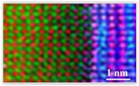
Superconducting and feromagnetic thin layers
A team of scientists lead by Prof. Bernhard Keimer, MPI for Solid State Research, and Dr. Eugen Weschke, HZB, have now investigated an artificial layer system composed of alternating nanolayers of YBaCuO and a ferromagnetic material. The thicknesses of the YBaCuO layers varied between 10 nm and 50 nm.
Tiny collective modulations of valence electrons observed
As interfaces often determine the properties of such heterostructures, physicists were particularly interested in their role for the present system. During his PhD work using resonant x-ray diffraction at BESSY II, Alex Frano could detect tiny collective modulations of valence electrons around Cu atoms in the YBaCuO layer. Data analysis revealed that the resulting charge density wave does not remain located close to the interface but extends across the whole layer. “ This finding is quite a surprise, as previous studies revealed a strong tendency of superconductivity to suppress the formation of charge density waves”, explains Frano.
Charge density wave is stabilized
“Engineering artifical interfaces in heterostructures of ferromagnetic and superconducting layers allowed to stabilize charge density waves even in the presence of superconductivity: YBaCuO remains superconducting, while the charges arrange in a periodic structure”, explains Weschke, “exploring the details of this coexistence on a microscopic scale is a challenging task for future experiments.” A most exciting perspective of the present results is paving the way to controlling the superconducting state itself.
Share on:


Suggested Items
Designer’s Notebook: What Designers Need to Know About Manufacturing, Part 2
04/24/2024 | Vern Solberg -- Column: Designer's NotebookThe printed circuit board (PCB) is the primary base element for providing the interconnect platform for mounting and electrically joining electronic components. When assessing PCB design complexity, first consider the component area and board area ratio. If the surface area for the component interface is restricted, it may justify adopting multilayer or multilayer sequential buildup (SBU) PCB fabrication to enable a more efficient sub-surface circuit interconnect.
Insulectro’s 'Storekeepers' Extend Their Welcome to Technology Village at IPC APEX EXPO
04/03/2024 | InsulectroInsulectro, the largest distributor of materials for use in the manufacture of PCBs and printed electronics, welcomes attendees to its TECHNOLOGY VILLAGE during this year’s IPC APEX EXPO at the Anaheim Convention Center, April 9-11, 2024.
ENNOVI Introduces a New Flexible Circuit Production Process for Low Voltage Connectivity in EV Battery Cell Contacting Systems
04/03/2024 | PRNewswireENNOVI, a mobility electrification solutions partner, introduces a more advanced and sustainable way of producing flexible circuits for low voltage signals in electric vehicle (EV) battery cell contacting systems.
Heavy Copper PCBs: Bridging the Gap Between Design and Fabrication, Part 1
04/01/2024 | Yash Sutariya, Saturn Electronics ServicesThey call me Sparky. This is due to my talent for getting shocked by a variety of voltages and because I cannot seem to keep my hands out of power control cabinets. While I do not have the time to throw the knife switch to the off position, that doesn’t stop me from sticking screwdrivers into the fuse boxes. In all honesty, I’m lucky to be alive. Fortunately, I also have a talent for building high-voltage heavy copper circuit boards. Since this is where I spend most of my time, I can guide you through some potential design for manufacturability (DFM) hazards you may encounter with heavy copper design.
Trouble in Your Tank: Supporting IC Substrates and Advanced Packaging, Part 5
03/19/2024 | Michael Carano -- Column: Trouble in Your TankDirect metallization systems based on conductive graphite or carbon dispersion are quickly gaining acceptance worldwide. Indeed, the environmental and productivity gains one can achieve with these processes are outstanding. In today’s highly competitive and litigious environment, direct metallization reduces costs associated with compliance, waste treatment, and legal issues related to chemical exposure. What makes these processes leaders in the direct metallization space?