


 The Right Approach: I Hear the Train A Comin'
 It’s Only Common Sense: OCCAM—the Time Is Now
 Marcy's Musings: The Growing Industry
Proper Breeding Ground for Germanene
June 27, 2016 | University of TwenteEstimated reading time: 2 minutes
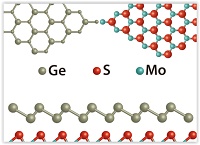
Graphene may currently be the best known ‘two dimensional’ material, its new cousin germanene seems to have properties that are even more attractive for application in electronics. For this, germanene has to grow in a one atom layer on top of a proper carrier - substrate. Scientists of the MESA+ Institute for Nanotechnology of the University of Twente managed to grow germanene on a semiconductor material, preserving the unique properties.
Germanene is a one atom thick sheet of germanium, in a honeycomb structure. It has clear similarities with graphene, the material that induced massive research activity worldwide, especially after 2010’s Nobel Prize. A major difference between graphene and germanene is the ‘band gap’, a property well-known in semiconductor electronics: thanks to this ‘jump’ of energy levels that electrons are allowed to have, it is possible to control, switch and amplify currents. Graphene had a very small band gap that can only be measured at very low temperatures, germanene shows a band gap that is significantly larger. Previous attempts to grow germanene, however, show that these attractive properties seem to vanish when it is grown on a metal surface: a good conductor of current. To prevent this, the UT scientists chose the semiconductor MoS2 as the substrate material.
Islands
Under ultra-high vacuum conditions, germanene indeed grows on the semiconductor. At first, the scientists observed islands at the locations where MoS2 had crystal defects, after that the germanene is spreading out covering a larger surface. An exciting question is, if the desired properties remain intact. First measurements show that the typical 2D properties and band gap are present, further low temperature measurements are needed to confirm that germanene operates in the desired way: the inner part would work as an insulator, while conducting channels are formed at the edges.
Sandwich
The other UT scientists did quantum mechanical calculations on the molybdenum-disulfide combination. They, for example, looked at the direction of growth, to be able to optimize the process. The theoretical group went one step further, by not only investigating the bilayer of molybdenum-disulfide, but als covering the germane with molybdeendisulfide. This prevents germanene from rapid oxidation. Calculations show that the sandwich construction has even better performance when it comes to the band gap.
Both publications show dat germanene, grown on molybdenum-disulfide is an important first step towards new electronic devices or unsuspected combinations with conventional devices. ‘Spintronics’, based on the spin movement of electrons, seems to be an attractive application area for germanene. Electrons with spin up and electrons with spin down have separate conducting channels on the edges of germanene. Harold Zandvliet recently received a grant for further research on this promising effect.
Share on:


Suggested Items
SMC Korea 2024 to Highlight Semiconductor Materials Trends and Innovations on Industry’s Path to $1 Trillion
04/24/2024 | SEMIWith Korea a major consumer of semiconductor materials and advanced materials a key driver of innovation on the industry’s path to $1 trillion, industry leaders and experts will gather at SMC (Strategic Materials Conference) Korea 2024 on May 29 at the Suwon Convention Center in Gyeonggi-do, South Korea to provide insights into the latest materials developments and trends. Registration is open.
Aaron Woolf, Dylan Peterson Join SIA Team
04/22/2024 | SIAThe Semiconductor Industry Association (SIA) announced Aaron Woolf and Dylan Peterson have joined the SIA team. Woolf will serve as director of global policy for economic security and Peterson will be a communications associate. SIA represents 99% of the U.S. semiconductor industry by revenue and nearly two-thirds of non-U.S. chip firms.
Digitalisation and ESG
04/19/2024 | Marina Hornasek-Metzl, AT&SDigitalisation and ESG are prominent and high-priority topics in the global business community. The first focuses on applying technology throughout the value chain to produce faster, smarter, and more desirable business outcomes. The latter emphasises the broader value a business is expected to create for its stakeholders from an environmental, social, and governance perspective.
SEMI Applauds CHIPS Program Office Progress to Diversify U.S. Semiconductor Industry Workforce
04/18/2024 | SEMIThe SEMI Foundation, the arm of SEMI dedicated to supporting economic opportunity for workers and the sustained growth of the microelectronics industry by creating pathways and opportunities for job seekers, applauded strides made by the CHIPS Program Office to diversify the U.S. semiconductor industry workforce and its release of the First Annual Report Regarding the Opportunities and Inclusion Activities Undertaken by the Department of Commerce.
Aspocomp’s Q1 Net Sales and Operating Result Decreased YoY
04/18/2024 | AspocompInflation and interest rates, weak economic development, the uncertainties posed by Russia’s war of aggression and the situation in the Middle East, and global trade policy tensions will affect the operating environment of Aspocomp and its customers in the 2024 fiscal year.