


 The Right Approach: I Hear the Train A Comin'
 It’s Only Common Sense: OCCAM—the Time Is Now
 Marcy's Musings: The Growing Industry
Watering Solar Cells Makes Them Grow… in Power!
July 27, 2016 | OISTEstimated reading time: 3 minutes
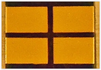
Perovskite solar cells are the rising star in the photovoltaic landscape. Since their invention, less than ten years ago, their efficiency has doubled twice and it is now over 22% – an astonishing result in the renewable energy sector. Taking the name ‘perovskite’ from the light-harvesting layer that characterizes them, these solar cells are lighter, cheaper, and more flexible than the traditional crystalline silicon-based cells.
Perovskite solar cells are usually exposed to ambient air for several hours after fabrication. This procedure increases their efficiency, even if the reason behind the phenomenon was unclear. The scientific explanation of this practice has now been discovered by researchers from the Energy Materials and Surface Sciences Unit (EMSS) at the Okinawa Institute of Science and Technology Graduate University (OIST) led by Prof Yabing Qi. Their results are published in Advanced Materials Interfaces.
“It’s intriguing: why do we need ambient air to enhance the effectiveness of perovskite solar cells?” Zafer Hawash, first author of the study and an OIST PhD student, commented. “Which component of the ambient air is linked to this phenomenon?” Starting from these questions, the researchers focused their attention on the top layer of the solar cells.
The choice was logical, because even if perovskite solar cell contains several layers – all of which may play a role in the cell efficiency – the top-most layer is the one in direct contact with ambient air. Thus, that is the layer most likely affected by the external environment. The layer is called ‘hole transport layer’, and it has a dopant, which is a substance that enhances the electrical conductivity of the material. “It is known that the dopant of the hole transport layer plays a key role in perovskite solar cells’ performance,” Hawash said. “But it was not clear how.”
The scientists performed controlled exposure of the hole transport layer to environmental gasses, focusing on oxygen, nitrogen, and moisture – water that is in a gas state. Then, they checked the electrical properties of the hole transport layer, using a variety of methods, to see if and how the inside of the transport layer changed. “What we found is that oxygen and nitrogen do not have any role in the redistribution of the dopants,” Hawash explained. “But in the case of moisture, the solar cells’ efficiency increases. This is the discovery: moisture is the air component that causes the redistribution of the dopant across the material, and thus the enhancement of the electric properties of the solar cells.”
The scientists explain this phenomenon with the structure of the transport layer, which has many pinholes that allow the passage of gasses between the ambient and the underneath material. The dopant in the transport layer is a salt – Lithium TFSI. Being a salt, the dopant has a hygroscopic nature: it absorbs water. When the solar cells are exposed to moisture, the water absorbed by the transport layer causes the dopant to redistribute. However, long time exposure to moisture has a detrimental effect on the solar cells.
During their experiments, the researchers were also able to document the role of oxygen in the solar cells’ performance. “Oxygen enhances the electrical conductivity of the transport layer as well, but this effect does not last long,” Hawash commented. “But with the right amount of exposure to moisture, the electric proprieties are irreversibly enhanced.”
Exposing the device to moisture after fabrication is then the most effective way to enhance the solar cells’ performance. Counterintuitively, then, water is what you need to have a perovskite solar cell that works properly. This finding is of high importance for the perovskite solar cells’ future, as it finally explains a common practice whose effectiveness was mostly anecdotic, and thus could now lead the way to further improvement in the perovskite solar cells’ performance.
Share on:


Suggested Items
Designer’s Notebook: What Designers Need to Know About Manufacturing, Part 2
04/24/2024 | Vern Solberg -- Column: Designer's NotebookThe printed circuit board (PCB) is the primary base element for providing the interconnect platform for mounting and electrically joining electronic components. When assessing PCB design complexity, first consider the component area and board area ratio. If the surface area for the component interface is restricted, it may justify adopting multilayer or multilayer sequential buildup (SBU) PCB fabrication to enable a more efficient sub-surface circuit interconnect.
Happy’s Tech Talk #27: Integrated Mesh Power System (IMPS) for PCBs
04/08/2024 | Happy Holden -- Column: Happy’s Tech TalkA significant decrease in HDI substrate production cost can be achieved by reducing the number of substrate layers from conventional through-hole multilayers and microvia multilayers of eight, 10, 12, and more to only two layers. Besides reducing direct processing steps, the yield will increase as defect-producing operations are eliminated. The integrated mesh power system (IMPS) was invented in the latter years of MCM-D use for thin-film fabrication. Those geometries fit today into our use of ultra HDI.
Insulectro’s 'Storekeepers' Extend Their Welcome to Technology Village at IPC APEX EXPO
04/03/2024 | InsulectroInsulectro, the largest distributor of materials for use in the manufacture of PCBs and printed electronics, welcomes attendees to its TECHNOLOGY VILLAGE during this year’s IPC APEX EXPO at the Anaheim Convention Center, April 9-11, 2024.
Now Available: Episode 4, Season 2 of Designing for Reality—Lamination
04/04/2024 | I-Connect007I-Connect007 has just released the latest episode of its podcast series, On the Line With..., which focuses on designing for reality in the electronics industry. Multilayer boards bring along a completely different set of processes. In this installment, ASC Sunstone VP/Manager Matt Stevenson discusses manufacturing techniques for multilayer boards. Of course, this necessitates a review of drill and registration techniques, followed by the ins and outs of lamination.
Heavy Copper PCBs: Bridging the Gap Between Design and Fabrication, Part 1
04/01/2024 | Yash Sutariya, Saturn Electronics ServicesThey call me Sparky. This is due to my talent for getting shocked by a variety of voltages and because I cannot seem to keep my hands out of power control cabinets. While I do not have the time to throw the knife switch to the off position, that doesn’t stop me from sticking screwdrivers into the fuse boxes. In all honesty, I’m lucky to be alive. Fortunately, I also have a talent for building high-voltage heavy copper circuit boards. Since this is where I spend most of my time, I can guide you through some potential design for manufacturability (DFM) hazards you may encounter with heavy copper design.