


 The Right Approach: I Hear the Train A Comin'
 It’s Only Common Sense: OCCAM—the Time Is Now
 Marcy's Musings: The Growing Industry
Are Carbon Nanotubes the next In-line for the Manufacture of Wearable Electronics?
September 6, 2016 | Taylor & FrancisEstimated reading time: 2 minutes
Carbon nanotubes show potential, but also many challenges, for the manufacture of flexible, wearable electronics, according to a research review in Science and Technology of Advanced Materials (Carbon nanotube based transparent conductive films: progress, challenges, and perspectives).
Scientists are developing flexible, stretchable and wearable optoelectronic devices, such as body sensors that could provide continuous monitoring of a person’s blood pressure. However, the jury is still out on the best materials to use for manufacturing these devices. Carbon nanotubes (CNTs) show promise and some challenges.
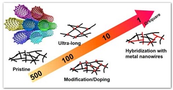
Ying Zhou and Reiko Azumi from Japan’s National Institute of Advanced Industrial Science and Technology reviewed the latest research on the use of carbon nanotubes in manufacturing an important component of optoelectronic devices called transparent conductive films (TCFs). These are thin films of a material that is optically transparent and electrically conductive. The market for TCFs is expected to reach 1.2 billion dollars by 2025. Currently, they are manufactured using indium tin oxide (ITO), which has the advantage of excellent electrical conductive properties but the disadvantage of poor flexibility, making it unsuitable for wearable devices.
Researchers are investigating several ITO alternatives for manufacturing TCFs. Carbon nanotube-based devices are among those showing promise. CNTs are nanosized cylindrical tubes with high theoretical electrical conductivity. CNTs have dropped in price due to their commercialization for applications such as water filtration systems, sports equipment, and batteries and conductors, for example, and prices could be further reduced by improving manufacturing processes.
Sensing devices, such as wearable touch panels, are the most promising application for CNT-based transparent conductive films. Two companies in Japan are already using CNTs to manufacture touch panels for mobile electronics. Organic LEDs (OLEDs), which are already used to manufacture thinner, lighter and more efficient TV screens, are another promising application for CNT-based TCFs. But other materials used in their manufacture, such as metal nanowires, have higher conductivity and transparency and thus result in a better performance.
“Based on the overview of the fabrication, properties and possible applications of CNT-based TCFs, it can be concluded that current CNT-based TCFs still do not meet the demands of performance/cost for industrial use,” write the researchers in their review published in the journal Science and Technology of Advanced Materials. Manufacturing costs need to be reduced while their conductivity and transparency need to be improved, they say.
The researchers recommend future investigations build on the flexibility and stretchability of CNT-based TCFs by improving their manufacturing and conductivity to make them worthy contenders for wearable optoelectronics.
Share on:


Suggested Items
Real Time with… IPC APEX EXPO 2024: Tools, Training, and Trends in Manufacturing Engineering
04/25/2024 | Real Time with...IPC APEX EXPOGuest Editor Kelly Dack and Product Specialist Erik Bateham of Polar Instruments discuss Polar's latest technology, including their role in aiding manufacturing engineers. They highlight the advanced capabilities of Polar's tools and the critical role of signal integrity analysis, as well as the importance of accurate modeling in board manufacturing. Polar's unique training approach and demonstration contact details are also explored.
TTM Celebrates the Grand Opening of Its First Manufacturing Facility in Penang
04/25/2024 | TTM Technologies, Inc.TTM Technologies, Inc., a leading global manufacturer of technology solutions including mission systems, radio frequency (RF) components and RF microwave/microelectronic assemblies, and quick-turn and technologically advanced printed circuit boards (PCBs), officially opened its first manufacturing plant in Penang, Malaysia with an investment of USD200 million (approximately RM958 million).
Listen Up! The Intricacies of PCB Drilling Detailed in New Podcast Episode
04/25/2024 | I-Connect007In episode 5 of the podcast series, On the Line With: Designing for Reality, Nolan Johnson and Matt Stevenson continue down the manufacturing process, this time focusing on the post-lamination drilling process for PCBs. Matt and Nolan delve into the intricacies of the PCB drilling process, highlighting the importance of hole quality, drill parameters, and design optimization to ensure smooth manufacturing. The conversation covers topics such as drill bit sizes, aspect ratios, vias, challenges in drilling, and ways to enhance efficiency in the drilling department.
Elevating PCB Design Engineering With IPC Programs
04/24/2024 | Cory Blaylock, IPCIn a monumental stride for the electronics manufacturing industry, IPC has successfully championed the recognition of the PCB Design Engineer as an official occupation by the U.S. Department of Labor (DOL). This pivotal achievement not only underscores the critical role of PCB design engineers within the technology landscape, but also marks the beginning of a transformative journey toward nurturing a robust, skilled workforce ready to propel our industry into the future.
Fujitsu, METRON Collaborate to Drive ESG Success
04/24/2024 | JCN NewswireFujitsu Limited and METRON SAS, a French cleantech company specializing in energy management solutions for industrial decarbonization, today announced a strategic initiative to contribute to the realization of carbon neutrality in the manufacturing industry.