


 The Right Approach: I Hear the Train A Comin'
 It’s Only Common Sense: OCCAM—the Time Is Now
 Marcy's Musings: The Growing Industry
Mexican Scientist in the Netherlands Seeks to Achieve Data Transmission
September 22, 2016 | Alpha GalileoEstimated reading time: 2 minutes
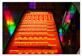
The photonic integrated circuits could replace electronic, currently used in computers or smartphones, to make them faster and compact.
In order to create effective technology that provides competitive in the market for data transmission, the mexican engineer Aura Higuera Rodriguez works in the design, manufacture and testing of dedicated optical interconnection between chips nanolasers, which ensures low power consumption and quick communication between them for sending information.
These are devices that can measure up to 300 nanometers in length, which consume low power, ie that do not generate excessive heat such as electronic devices made from silicon. "Those who we created are capable of supporting light sources and transmit data at high speed”, explained Aura Rodriguez, a doctoral student in Photonic Integration at the Technical University of Eindhoven in the Netherlands.
A single chip can contain hundreds of thousands of devices, they can be nanolasers, receivers or transmitters. These nanolasers be adapted in optical interconnects within a single chip, for example in the central processing unit of a computer or a smartphone, the purpose is to generate quick communication between chips to send information. The next generation of devices, the era of photonics.
"When we produce is like playing with a block of modeling clay, that is what we cut and molded to create and shape the laser. We ended up forming similar blocks to the lego, who put them together forms a data transmission system that uses light to carry information at high speed”, said the Telecommunications engineer from UNAM.
Is worth highlighting that these lasers are not yet marketed in the world, because, among other things, premature state in which has not reached a performance of high efficiency, difficulty in manufacturing and handling of physical properties of materials, and processing that is delicate because they are toxic materials; however, the large telecommunications companies have already announced that they will change their mode of operation to photonics, ie invest in the development of this technology because electronics no longer be viable in the future to meet the need for data transmission more speed.
Currently the investigation is under development and continuous study. "At the moment have made a chip with nanolasers, we must now characterize and check if it works technologically and then integrate it with other functions”, explained.
Despite being technology and very expensive in Mexico may apply. "You can create designs chips using specialized software, sent to Europe to manufacture and characterize a given that the necessary equipment is not expensive as used for manufacturing laboratory. It really is possible, photonics has niche opportunity and development in Mexico, you only need to start generating cooperation and seek opportunities for projects at universities and research institutes and development to consider working with technology ".
Share on:


Suggested Items
Warm Windows and Streamlined Skin Patches – IDTechEx Explores Flexible and Printed Electronics
04/26/2024 | IDTechExFlexible and printed electronics can be integrated into cars and homes to create modern aesthetics that are beneficial and easy to use. From luminous car controls to food labels that communicate the quality of food, the uses of this technology are endless and can upgrade many areas of everyday life.
iNEMI Packaging Tech Topic Series: Role of EDA in Advanced Semiconductor Packaging
04/26/2024 | iNEMIAdvanced semiconductor packaging with heterogenous integration has made on-package integration of multiple chips a crucial part of finding alternatives to transistor scaling. Historically, EDA tools for front-end and back-end design have evolved separately; however, design complexity and the increased number of die-to-die or die-to-substrate interconnections has led to the need for EDA tools that can support integration of overall design planning, implementation, and system analysis in a single cockpit.
Koh Young Showcases Award-winning Inspection Solutions at SMTconnect with SmartRep in Hall 4A.225
04/25/2024 | Koh Young TechnologyKoh Young Technology, the industry leader in True 3D measurement-based inspection solutions, will showcase an array of award-winning inspection and measurement solutions at SMTconnect alongside its sales partner, SmartRep, in booth 4A.225 at NürnbergMesse from June 11-13, 2023. The following offers a glimpse into what Koh Young will present at the tradeshow:
Real Time with… IPC APEX EXPO 2024: Plasmatreat: Innovative Surface Preparation Solutions
04/25/2024 | Real Time with...IPC APEX EXPOIn this interview, Editor Nolan Johnson speaks with Hardev Grewal, CEO and president of Plasmatreat, a developer of atmospheric plasma solutions. Plasmatreat uses clean compressed air and electricity to create plasma, offering environmentally friendly methods for surface preparation. Their technology measures plasma density for process optimization and can remove organic micro-contamination. Nolan and Hardev also discuss REDOX-Tool, a new technology for removing metal oxides.
Nanotechnology Market to Surpass $53.51 Billion by 2031
04/25/2024 | PRNewswireSkyQuest projects that the nanotechnology market will attain a value of USD 53.51 billion by 2031, with a CAGR of 36.4% over the forecast period (2024-2031).