


 The Right Approach: I Hear the Train A Comin'
 It’s Only Common Sense: OCCAM—the Time Is Now
 Marcy's Musings: The Growing Industry
Direct Observation of Graphene Decoupling on Cu
September 23, 2016 | UNISTEstimated reading time: 2 minutes
The graphene films, grown on the copper (Cu) substrates must be detached clean without leaving residue behind, as residual metallic impurities can significantly alter electronic and electrochemical properties of graphene.
However, thanks to recent advances in graphene transfer method, the electrochemical corrosion of graphene coatings on Cu has allowed the monolayer-thick material to be mechanically delaminated without significantly compromising its structural integrity.
The new UNIST graphene research veers off in a new direction by succesfully seperating graphene from its metal growth substrates without the assistance of the adhesive tape. The research findings have been published in the August issue of the Journal of the American Chemical Society (JACS).
In the study, led by Prof. Sang Kyu Kwak (School of Energy and Chemical Engineering, UNIST) and Prof. Rodney Ruoff (Center for Multidimensional Carbon Materials, IBS), the research team revealed the surface oxidation chemistry of the nanoribbon-covered Cu(111) surface.
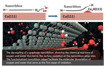
The decoupling of a graphene nanoribbon, showing the chemical reactions of oxygen and water that led to the surface oxidation at the nanoribbon edge sites. The functionalized nanoribbon edges facilitate the molecular dissociation of oxygen and water that serve as the first stage of oxidation.
Specifically, they have demonstrated that the graphene nanoribbon (GNR) edge type influences the initial oxidation stages of the Cu surface, thus driving the nanoribbon decoupling by the intercalation of surrounding adsorbate molecules (e.g. oxygen and water).
The difference between the armchair GNR and zigzag GNR on the Cu(111) substrate, is distinguished by the presence of an edge state in the zigzag GNR edges, which has been attributed to the hybridization between the out-of-plane carbon π orbitals and the metal d orbitals. This edge state, however, is absent in the armchair GNR edge atoms. Such an observation has not been reported for H-terminated GNR on Cu(111).
Vibrational stretching mode calculations showed that the GNR edges influenced the molecular adsorption of oxygen at the bare and GNR/Cu sites, confirming the role of GNR edges in weakening the pre-elongated O-O bond at the GNR/Cu interface. The research team also explained that the GNR edges facilitated the stabilization of water molecules (regardless of surface oxygenation), which would otherwise be unstable on the bare Cu surface.
Dr. Kester Wong, who takes full charge of the research, notes that “GNR-mediated interactions between water and the chemisorbed oxygen radicals can shed further light in elucidating the role of water and oxygen in the surface oxide formation.”
“This particular study may have interesting implications for the development of regioselective graphene-based catalysis. Nonetheless, employing other crystal facets for the interfacial study of low dimensional materials is of great interest, and several investigations are being heavily pursued by our group in this area”, says Prof. Kwak.
This work has been supported by Institute of Basic Sciences (IBS, CMCM) and Basic Science Research Program through the National Research Foundation of Korea (NRF), funded by the Korean Ministry of Science, ICT & Future Planning (MSIP).
Share on:


Suggested Items
Designer’s Notebook: What Designers Need to Know About Manufacturing, Part 2
04/24/2024 | Vern Solberg -- Column: Designer's NotebookThe printed circuit board (PCB) is the primary base element for providing the interconnect platform for mounting and electrically joining electronic components. When assessing PCB design complexity, first consider the component area and board area ratio. If the surface area for the component interface is restricted, it may justify adopting multilayer or multilayer sequential buildup (SBU) PCB fabrication to enable a more efficient sub-surface circuit interconnect.
Insulectro’s 'Storekeepers' Extend Their Welcome to Technology Village at IPC APEX EXPO
04/03/2024 | InsulectroInsulectro, the largest distributor of materials for use in the manufacture of PCBs and printed electronics, welcomes attendees to its TECHNOLOGY VILLAGE during this year’s IPC APEX EXPO at the Anaheim Convention Center, April 9-11, 2024.
ENNOVI Introduces a New Flexible Circuit Production Process for Low Voltage Connectivity in EV Battery Cell Contacting Systems
04/03/2024 | PRNewswireENNOVI, a mobility electrification solutions partner, introduces a more advanced and sustainable way of producing flexible circuits for low voltage signals in electric vehicle (EV) battery cell contacting systems.
Heavy Copper PCBs: Bridging the Gap Between Design and Fabrication, Part 1
04/01/2024 | Yash Sutariya, Saturn Electronics ServicesThey call me Sparky. This is due to my talent for getting shocked by a variety of voltages and because I cannot seem to keep my hands out of power control cabinets. While I do not have the time to throw the knife switch to the off position, that doesn’t stop me from sticking screwdrivers into the fuse boxes. In all honesty, I’m lucky to be alive. Fortunately, I also have a talent for building high-voltage heavy copper circuit boards. Since this is where I spend most of my time, I can guide you through some potential design for manufacturability (DFM) hazards you may encounter with heavy copper design.
Trouble in Your Tank: Supporting IC Substrates and Advanced Packaging, Part 5
03/19/2024 | Michael Carano -- Column: Trouble in Your TankDirect metallization systems based on conductive graphite or carbon dispersion are quickly gaining acceptance worldwide. Indeed, the environmental and productivity gains one can achieve with these processes are outstanding. In today’s highly competitive and litigious environment, direct metallization reduces costs associated with compliance, waste treatment, and legal issues related to chemical exposure. What makes these processes leaders in the direct metallization space?