


 The Right Approach: I Hear the Train A Comin'
 It’s Only Common Sense: OCCAM—the Time Is Now
 Marcy's Musings: The Growing Industry
Mysterious Quantum Properties in Material Point to New Applications in Electronics
September 26, 2016 | Lawrence Berkeley National LaboratoryEstimated reading time: 5 minutes
Researchers have created an exotic 3-D racetrack for electrons in ultrathin slices of a nanomaterial they fabricated at the Department of Energy’s Lawrence Berkeley National Laboratory (Berkeley Lab).
The international team of scientists from Berkeley Lab, UC Berkeley, and Germany observed, for the first time, a unique behavior in which electrons rotate around one surface, then through the bulk of the material to its opposite surface and back.
The possibility of developing so-called “topological matter” that can carry electrical current on its surface without loss at room temperature has attracted significant interest in the research community. The ultimate goal is to approach the lossless conduction of another class of materials, known as superconductors, but without the need for the extreme, freezing temperatures that superconductors require.
“Microchips lose so much energy through heat dissipation that it’s a limiting factor,” said James Analytis, a staff scientist at Berkeley Lab and assistant professor of physics at UC Berkeley who led the study, published in Nature. “The smaller they become, the more they heat up.”
The studied material, an inorganic semimetal called cadmium arsenide (Cd3As2), exhibits quantum properties—which are not explained by the classical laws of physics—that offer a new approach to reducing waste energy in microchips. In 2014, scientists discovered that cadmium arsenide shares some electronic properties with graphene, a single-atom-thick material also eyed for next-generation computer components, but in a 3-D form.
“What’s exciting about these phenomena is that, in theory, they are not affected by temperature, and the fact they exist in three dimensions possibly makes fabrication of new devices easier,” Analytis said.
The cadmium arsenide samples displayed a quantum property known as “chirality” that couples an electron’s fundamental property of spin to its momentum, essentially giving it left- or right-handed traits. The experiment provided a first step toward the goal of using chirality for transporting charge and energy through a material without loss.
In the experiment, researchers manufactured and studied how electric current travels in slices of a cadmium arsenic crystal just 150 nanometers thick, or about 600 times smaller than the width of a human hair, when subjected to a high magnetic field.
The crystal samples were crafted at Berkeley Lab’s Molecular Foundry, which has a focus in building and studying nanoscale materials, and their 3-D structure was detailed using X-rays at Berkeley Lab’s Advanced Light Source.
Many mysteries remain about the exotic properties of the studied material, and as a next step researchers are seeking other fabrication techniques to build a similar material with built-in magnetic properties, so no external magnetic field is required.
“This isn’t the right material for an application, but it tells us we’re on the right track,” Analytis said.
If researchers are successful in their modifications, such a material could conceivably be used for constructing interconnects between multiple computer chips, for example, for next-generation computers that rely on an electron’s spin to process data (known as “spintronics”), and for building thermoelectric devices that convert waste heat to electric current.
It wasn’t clear at first whether the research team would even be able to manufacture a pure enough sample at the tiny scale required to carry out the experiment, Analytis said.
“We wanted to measure the surface states of electrons in the material. But this 3-D material also conducts electricity in the bulk—it’s central region—as well as at the surface,” he said. As a result, when you measure the electric current, the signal is swamped by what is going on in the bulk so you never see the surface contribution.”
So they shrunk the sample from millionths of a meter to the nanoscale to give them more surface area and ensure that the surface signal would be the dominant one in an experiment.
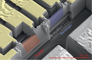
This image, produced by a scanning electron microscope, shows three sheets of a crystal material called cadmium arsenide. The finely polished rectangular sheets (purple) were sliced from the same crystal in varying thicknesses. They measure about 4 microns (thousandths of a millimeter) tall by 10 microns wide.
Page 1 of 2
Share on:


Suggested Items
Real Time with... IPC APEX EXPO 2024: Sustainability in the Industry
04/26/2024 | Real Time with...IPC APEX EXPOGuest Editor Henry Crandall and Chris Nash of Indium Corporation discuss the company's 90th anniversary and its focus on sustainability. They focus on the benefits of sustainable materials, their compatibility, and value propositions. The conversation also highlights how Durafuse LT technology's role in reducing reflow temperatures is leading to significant cost and energy savings. Nash also touches on downstream sustainability efforts such as using recycled materials for packaging.
SMC Korea 2024 to Highlight Semiconductor Materials Trends and Innovations on Industry’s Path to $1 Trillion
04/24/2024 | SEMIWith Korea a major consumer of semiconductor materials and advanced materials a key driver of innovation on the industry’s path to $1 trillion, industry leaders and experts will gather at SMC (Strategic Materials Conference) Korea 2024 on May 29 at the Suwon Convention Center in Gyeonggi-do, South Korea to provide insights into the latest materials developments and trends. Registration is open.
Groundbreaking Ceremony Marks the Beginning of a New Era for Newccess Industrial; The Construction of the MINGXIN Building
04/12/2024 | Newccess IndustrialOn a clear and sunny day in March, the groundbreaking ceremony for the MINGXIN Building took place in Shenzhen, China. This moment marked the official commencement of construction for a project that will reshape the semiconductor materials industry.
The Need for a Holistic Global Sustainability Standard
04/10/2024 | Michael Ford, Aegis SoftwareNo one can deny that the resources of our fragile planet are finite. The environment seems like a third party, subject to constant degradation. We’re acutely aware of the effects of pollution on our climate, and despite our “throw-away” culture, recycling and recovery of materials has remained relatively expensive, even as we use more energy just to survive.
iNEMI Publishes Four Roadmap Topics
04/04/2024 | iNEMIThe International Electronics Manufacturing Initiative (iNEMI) announces the availability of the first roadmap topics in the new iNEMI Roadmap format. Printed circuit boards, sustainable electronics, smart manufacturing, and mmWave materials and test are now available online.