


 The Right Approach: I Hear the Train A Comin'
 It’s Only Common Sense: OCCAM—the Time Is Now
 Marcy's Musings: The Growing Industry
A Record Photovoltaic Effect Observed in Antiferroelectrics
October 3, 2016 | ICN2Estimated reading time: 2 minutes
The photovoltaic effect is the main physical and chemical principle behind every photovoltaic device, more popular known as a Solar Cell. It is characterized by the conversion of photons (from any artificial or natural light source like sunlight) into usable electrical energy. Modern photovoltaic devices have been intensively researched since the early days of the semiconductor transistor revolution (1940s) and nowadays they provide around 13% of the global renewable electric energy, a figure that will steadily increase to meet the COP21 directives.
A fundamental limit of current photovoltaic devices –all of which are based on semiconductor junctions- is its output voltage, which typically is limited to ~ 1.5 volts (like AA battery) per junction. This limit is due to intrinsic material properties –basically, the semiconductor bandgap- and is therefore independent of the solar cell area, regardless whether it is a microscopic dot or a large area solar panel. .
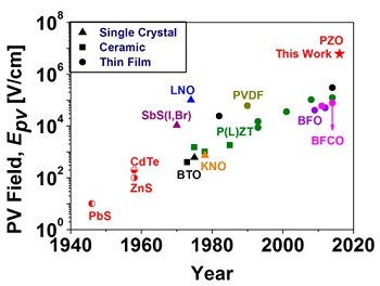
By contrast, there is another family of materials where photovoltages much larger than the bandgap can be achieved; they are the so-called ferroelectrics, intrinsically polar materials where the photovoltage is originated by the asymmetry of the crystal lattice instead of by a semiconductor interfacial effect. Until now, ferroelectric materials held the record for the highest photoelectric fields ever produced (the photovoltaic field is, in first approximation, the photovoltage divided by the thickness of the device).
Now, a multidisciplinary research team from the Institut Català de Nanociència i Nanotecnologia (ICN2), funded by Severo Ochoa Excellence Program, has reported in Advanced Materials the largest ever photovoltaic field, reaching values in excess of a million volt per centimetre and beating by a factor of x20 the previous state of the art. Furthermore they have discovered the effect in a class of materials (known as antiferroelectrics) where the photovoltaic effect had not been explored before. The ICN2 research team behind the discovery is formed by Dr Amador Pérez-Tomás from ICN2, Prof Mónica Lira-Cantú from CSIC and ICREA research professor Gustau Catalán.
It was in many ways a real surprise as these materials are antipolar and not polar (hence the name antiferroelectrics) and thus it was not expected to present stable photovoltaic action, but the authors have proposed an explanation for the observed results. There is, however, still some way for this discovery to be of practical use in photovoltaic cells, because even though their photovoltage is very large, their electrical current still remains too low, meaning that the electrical power is still below that of standard semiconductor devices. The researchers have nevertheless filled a patent to protect the technology, and are working on the optimization of the device to rapidly advance into practical applications as they believe it can find uses in practical applications such as photovoltaic sensors and photocatalysts.
Share on:


Suggested Items
Real Time with... IPC APEX EXPO 2024: Sustainability in the Industry
04/26/2024 | Real Time with...IPC APEX EXPOGuest Editor Henry Crandall and Chris Nash of Indium Corporation discuss the company's 90th anniversary and its focus on sustainability. They focus on the benefits of sustainable materials, their compatibility, and value propositions. The conversation also highlights how Durafuse LT technology's role in reducing reflow temperatures is leading to significant cost and energy savings. Nash also touches on downstream sustainability efforts such as using recycled materials for packaging.
SMC Korea 2024 to Highlight Semiconductor Materials Trends and Innovations on Industry’s Path to $1 Trillion
04/24/2024 | SEMIWith Korea a major consumer of semiconductor materials and advanced materials a key driver of innovation on the industry’s path to $1 trillion, industry leaders and experts will gather at SMC (Strategic Materials Conference) Korea 2024 on May 29 at the Suwon Convention Center in Gyeonggi-do, South Korea to provide insights into the latest materials developments and trends. Registration is open.
Groundbreaking Ceremony Marks the Beginning of a New Era for Newccess Industrial; The Construction of the MINGXIN Building
04/12/2024 | Newccess IndustrialOn a clear and sunny day in March, the groundbreaking ceremony for the MINGXIN Building took place in Shenzhen, China. This moment marked the official commencement of construction for a project that will reshape the semiconductor materials industry.
The Need for a Holistic Global Sustainability Standard
04/10/2024 | Michael Ford, Aegis SoftwareNo one can deny that the resources of our fragile planet are finite. The environment seems like a third party, subject to constant degradation. We’re acutely aware of the effects of pollution on our climate, and despite our “throw-away” culture, recycling and recovery of materials has remained relatively expensive, even as we use more energy just to survive.
iNEMI Publishes Four Roadmap Topics
04/04/2024 | iNEMIThe International Electronics Manufacturing Initiative (iNEMI) announces the availability of the first roadmap topics in the new iNEMI Roadmap format. Printed circuit boards, sustainable electronics, smart manufacturing, and mmWave materials and test are now available online.