


 The Right Approach: I Hear the Train A Comin'
 It’s Only Common Sense: OCCAM—the Time Is Now
 Marcy's Musings: The Growing Industry
Stanford Physicists Develop a More Sensitive Microscope
October 3, 2016 | Stanford UniversityEstimated reading time: 3 minutes
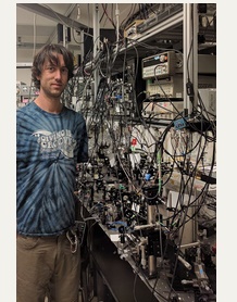
Anyone who has taken a photo in a poorly lit restaurant or dim concert venue knows all too well the grainy, fuzzy outcomes of low-light imaging. Scientists trying to take images of biological specimens encounter the same issue because they tend to work in low light to avoid damaging delicate samples. The resulting grainy images can make it hard to distinguish the intricate proteins and internal structures they are trying to study.
The effect that causes grainy images of either your meal or a biological sample is called shot noise. Stanford researchers may have come up with an elegant solution to this problem, which they refer to as “multi-pass microscopy.” This technique, detailed in a Sept. 27 paper in Nature Communications, could make it possible to view proteins and living cells in greater clarity than ever before.
“If you work at low-light intensities, shot noise limits the maximum amount of information you can get from your image,” said Thomas Juffmann, co-author of the research and a postdoctoral research fellow in Stanford Professor Mark Kasevich’s research group. “But there’s a way around that; the shot-noise limit is not fundamental.”
Recycled photons
In optical microscopy, individual units of light, called photons, strike a detector to make the image. The researchers have found they get better results if each photon interacts with the sample multiple times, even in low light. To implement this in a microscope, instead of sending light through a specimen and then directly capturing the resulting image, the Stanford team repeatedly reflects the image back onto the specimen.
“In a sense, it’s like you’re taking a picture of multiple times your object,” said co-author Brannon Klopfer, a graduate student in the Kasevich group. “You first take an image of the specimen, you then illuminate it with an image of itself, and the image you get, you again send back to illuminate the sample. This leads to contrast enhancement.”
Multi-pass microscopy is not the only approach to overcoming the shot-noise limit. Another method, called quantum microscopy, uses entangled photons to achieve the same result, but it is more challenging to carry out.
Entangled photons are photons that show quantum correlations. This means that performing an action on one of two entangled photons can have an effect on the other one, even if they are far apart from each other. It is what Albert Einstein referred to as “spooky action at a distance.”
The ability of entangled photons to give information about each other means that quantum microscopy can produce higher-quality images compared to standard microscopy. At present, multi-pass microscopy has the potential to create comparably enhanced results with the added benefit of requiring less arduous preparation than quantum microscopy.
“The advantage you gain when entangling two photons is what we gain when we go through the sample twice,” Juffmann said. “Currently, it is technologically easier to make a photon pass through a sample 10 times than to create a state in which 10 photons are entangled with each other.”
A general technique
Multi-pass microscopy could boost more than just low-light imaging because it acts as a general signal-enhancing technique. The method can increase the sensitivity of various microscopy techniques, so long as a source of image noise doesn’t build up with the recycling of photons.
“While multi-passing builds up the signal in your image, the noise is hardly affected,” Klopfer said.
At present, multi-passing is restricted to optical microscopes.But the team at Stanford is also working on multi-pass electron microscopy, where damage prevents the atomic-scale imaging of single proteins or DNA. Recycling the electrons in electron microscopy would improve image quality just as the recycling of photons does in the optical microscopes.
Share on:


Suggested Items
Inkjet Solder Mask ‘Has Arrived’
04/10/2024 | Pete Starkey, I-Connect007I was delighted to be invited to attend an interactive webinar entitled “Solder Mask Coating Made Easy with Additive Manufacturing,” hosted by SUSS MicroTec Netherlands in Eindhoven. The webinar was introduced and moderated by André Bodegom, managing director at Adeon Technologies, and the speakers were Mariana Van Dam, senior product manager PCB imaging solutions at AGFA in Belgium; Ashley Steers, sales manager at Electra Polymers in the UK; and Dr. Luca Gautero, product manager at SUSS MicroTec Netherlands.
NetVia Group Acquires Direct Imaging from Mivatek
04/09/2024 | Miva TechnologiesMiva Technologies is pleased to announce NetVia Group, Irving, TX has acquired a new Miva 2400NG Dual Tray Direct Imaging System with 30-micron capabilities for inner, outer and soldermask imaging.
Teledyne to Acquire Adimec
02/13/2024 | TeledyneTeledyne Technologies Incorporated announced that it has entered into an agreement to acquire Adimec Holding B.V. and its subsidiaries.
Real Time with... productronica 2023: MivaTek Global Advances Technology With High-res Imaging System
12/08/2023 | Real Time with...productronicaMivaTek's Brendan Hogan talks about how the company employs Digitally Adaptive Rasterization Technology (DART) in their high-res imaging equipment. He also shares how the blurred line between semiconductors and microelectronics is driving broader application of the imaging process.
Keysight Enables Validation of Arbe 4D Imaging Radar Chipset
11/30/2023 | Keysight Technologies, Inc.Keysight Technologies, Inc. announces that Arbe has selected the E8719A Radar Target Solution (RTS) to test the Arbe 4D imaging radar chipset for automotive applications.