


 The Right Approach: I Hear the Train A Comin'
 It’s Only Common Sense: OCCAM—the Time Is Now
 Marcy's Musings: The Growing Industry
Gentle Sensors for Diagnosing Brain Disorders
October 3, 2016 | KAUSTEstimated reading time: 2 minutes
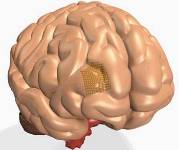
Flexible, low-cost sensor technology leading to safer and improved diagnoses and treatment of brain disorders has been developed by Saudi Arabia's King Abdullah University of Science and Technology (KAUST) scientists (Small, "Deterministic integration of out-of-plane sensor arrays for flexible electronic applications").
Mapping the electrical activity of the brain is critical in understanding neurological disorders, such as depression and Alzheimer’s disease. Currently, multielectrode arrays, called Michigan or Utah arrays, are used to monitor brain activity. Made from layers of conductive silicon needles, these rigid devices are inserted through the scalp to monitor the brain’s surface. The needles can cause inflammation of the tissues and so they must be removed within a year.
Muhammad Hussain and Aftab Hussain from the KAUST Integrated Nanotechnology Laboratory and Integrated Disruptive Electronic Applications Laboratory wanted to develop a soft and flexible sensor that could be placed on the surface of the brain within the intracranial space, providing better contact and reducing the risk of damage to tissues.
“Sensors require associated electronics to interface with us, and these electronics dissipate heat causing a burning effect in the brain which can permanently damage tissues,” explains Muhammad Hussain. “The challenge is to keep the electronics away from the brain.”
Working within these parameters, they fabricated a sensor made from gold electrodes encased in a polymer coating with their connections oriented vertically, and, by placing the connectors on top of the sensor and allowing them to pass through the polymer support, an integrated circuit (IC) could be attached to the flip side of the device, isolating it from the brain surface and preventing hotspots.
The intracranial space of the brain presents an area of only 64 cm2 for mapping more than 80 billion neurons, so not only is it safer to prevent the electronics from making contact with the brain, it also maximizes the number of neurons that can be monitored by the sensor array.
“The sensor is in contact with the soft tissues of the brain, where it collects activity data, and the IC is placed on top, with a soft insulating polymeric material separating them, allowing a larger area to be mapped and a reduction in the heating effect,” says Hussain.
By using state-of-the-art technology, used for fabricating integrated circuits, the researchers have developed a method that could lead to mass-produced sensors that are safer, have improved mapping capabilities, and are also robust enough for long lasting functionality.
“We are currently collaborating with Harvard-MIT Medical Institute on using the technique to improve the efficiency of the mapping interface system,” says Hussain.
Share on:


Suggested Items
Warm Windows and Streamlined Skin Patches – IDTechEx Explores Flexible and Printed Electronics
04/26/2024 | IDTechExFlexible and printed electronics can be integrated into cars and homes to create modern aesthetics that are beneficial and easy to use. From luminous car controls to food labels that communicate the quality of food, the uses of this technology are endless and can upgrade many areas of everyday life.
Book Excerpt: The Printed Circuit Assembler’s Guide to... Factory Analytics
04/24/2024 | I-Connect007 Editorial TeamIn our fast-changing, deeply competitive, and margin-tight industry, factory analytics can be the key to unlocking untapped improvements to guarantee a thriving business. On top of that, electronics manufacturers are facing a tremendous burden to do more with less. If you don't already have a copy of this book, what follows is an excerpt from the introduction chapter of 'The Printed Circuit Assembler’s Guide to... Factory Analytics: Unlocking Efficiency Through Data Insights' to whet your appetite.
Listen Up! The Intricacies of PCB Drilling Detailed in New Podcast Episode
04/25/2024 | I-Connect007In episode 5 of the podcast series, On the Line With: Designing for Reality, Nolan Johnson and Matt Stevenson continue down the manufacturing process, this time focusing on the post-lamination drilling process for PCBs. Matt and Nolan delve into the intricacies of the PCB drilling process, highlighting the importance of hole quality, drill parameters, and design optimization to ensure smooth manufacturing. The conversation covers topics such as drill bit sizes, aspect ratios, vias, challenges in drilling, and ways to enhance efficiency in the drilling department.
Elevating PCB Design Engineering With IPC Programs
04/24/2024 | Cory Blaylock, IPCIn a monumental stride for the electronics manufacturing industry, IPC has successfully championed the recognition of the PCB Design Engineer as an official occupation by the U.S. Department of Labor (DOL). This pivotal achievement not only underscores the critical role of PCB design engineers within the technology landscape, but also marks the beginning of a transformative journey toward nurturing a robust, skilled workforce ready to propel our industry into the future.
Winner of The Science Show Rakett 69 Receives Incap Scholarship
04/24/2024 | IncapThe winner of the Rakett 69 science show, Andri Türkson, who stood out as an electronics enthusiast, received a scholarship from Incap Estonia, along with an internship opportunity in Saaremaa.