


 The Right Approach: I Hear the Train A Comin'
 It’s Only Common Sense: OCCAM—the Time Is Now
 Marcy's Musings: The Growing Industry
Enhancing the Superconducting Properties of an Iron-based Material
October 7, 2016 | BNLEstimated reading time: 4 minutes
Iron-based superconductors can conduct electricity without resistance at unusually high temperatures relative to those of conventional superconductors, which must be chilled to near absolute zero (minus 459 degrees Fahrenheit) to release their superconducting powers. In addition, they're relatively easy to bend and can carry electrical current easily in different directions under high magnetic fields before superconductivity becomes suppressed. These characteristics make iron-based superconductors promising for advanced energy applications, from electric vehicles to wind turbines and medical imaging devices. However, the amount of current they can carry has been low in comparison to other superconductors. Scientists have been trying to increase this amount, but doing so has often come at the cost of degrading another key superconducting property--the critical temperature at which superconductivity emerges.
Now, a team of scientists has come up with a way to double the amount of electrical current an iron-based material can carry without losing its superconducting properties, while increasing the material's critical temperature. Their method, reported in a paper published today in Nature Communications ("A route for a strong increase of critical current in nanostrained iron-based superconductors"), makes use of a readily available technology that could be used to improve the performance of superconducting wires and tapes.
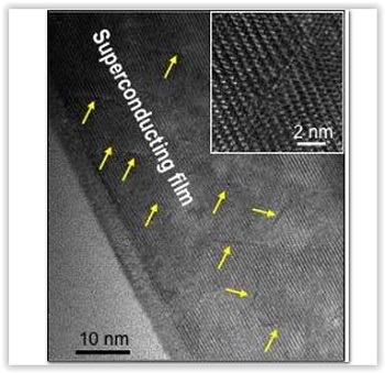
Superconducting Iron-Based Film
An electron microscope image of one of the team's superconducting iron-based films is shown after the scientists irradiated the film with low-energy protons shows the resulting chains of defects (indicated by yellow arrows). The inset image shows a zoomed-in view of a typical defect chain. (Image: Courtesy of the researchers)
"By bombarding the material with protons at low energy, we simultaneously increased the material's current-carrying capacity and critical temperature--the first time that this has been possible in an iron-based superconductor," said physicist Qiang Li, head of the Advanced Energy Materials Group at the U.S. Department of Energy's (DOE) Brookhaven National Laboratory, who directed the research. "There are low-energy ion facilities all over the world that can do this inexpensively."
Shooting ions at superconducting materials is a well-established method for artificially introducing defects in the crystal structure or chemistry of the materials to increase the amount of current they can carry. These defects "pin" in place, or trap, the microscopic magnetic vortices that form when the superconductor is placed in a strong magnetic field, such as those generated by magnets in magnetic resonance imaging (MRI) machines. If free to move around, the vortices dissipate energy, thereby destroying the superconductor's ability to carry electrical current without energy loss.
Unfortunately, if the defects produced by ion irradiation create too much disorder in the superconductor, they lower its critical temperature. Because superconductors currently require extreme cooling to conduct electricity without resistance, any decrease in the critical temperature is undesirable.
In a Goldilocks sense, the defects must be "just right"--not too big, not too small. Scientists can design such defects by selecting the appropriate ion species (e.g., protons, gold ions, argon ions) and ion energy.
"Some ions or energies may cause large enough damage to interfere with superconductivity, while others may not produce any effect at all," explained coauthor Toshinori Ozaki, a former scientist in Brookhaven Lab's Advanced Energy Materials Group who is now a faculty member at Japan's Kwansei Gakuin University. "So we run simulations to figure out what combination should produce the optimal defect--one that can hold down the magnetic vortices without negatively impacting the material's superconducting properties."
In the case of the iron-based material the team studied, low-energy protons did the trick. Using electron microscopes, the scientists took images of the thin films (about 100 nanometers thick) of the material they prepared, before and after they hit the films with low-energy protons.
"Throughout the irradiated films, we saw individual chains of defects created by the collisions between the incident ions and nucleus that broke the perfect atomic order, causing the lattice to locally compress or stretch out," said coauthor Lijun Wu, a materials scientist at Brookhaven who led the microscopy work.
In a performance check, the scientists measured the amount of electrical current running through the films in low and high magnetic fields. In high fields, the irradiated films carried more current than any low-temperature superconductor. This result suggests that the defects and local lattice strain must be strongly pinning the magnetic vortices that would otherwise impede the flow of current.
To figure out what caused the surprising increase in the critical temperature, the team created a strain "map" that laid out where the locally compressed and tensile (stretched out) regions were located. Previous studies had already shown that the type of lattice strain correlates with the critical temperature: highly compressed regions with a high critical temperature, and highly tensile regions with a low critical temperature. In the team's films, the compressive ones took up much more space, leading to an overall raised critical temperature.
According to Li, these performance gains are only the beginning: "We believe that the critical current and temperature can be further enhanced by fine tuning the structure of the defects and the arrangement of the lattice strains."
Share on:


Suggested Items
Real Time with... IPC APEX EXPO 2024: Sustainability in the Industry
04/26/2024 | Real Time with...IPC APEX EXPOGuest Editor Henry Crandall and Chris Nash of Indium Corporation discuss the company's 90th anniversary and its focus on sustainability. They focus on the benefits of sustainable materials, their compatibility, and value propositions. The conversation also highlights how Durafuse LT technology's role in reducing reflow temperatures is leading to significant cost and energy savings. Nash also touches on downstream sustainability efforts such as using recycled materials for packaging.
SMC Korea 2024 to Highlight Semiconductor Materials Trends and Innovations on Industry’s Path to $1 Trillion
04/24/2024 | SEMIWith Korea a major consumer of semiconductor materials and advanced materials a key driver of innovation on the industry’s path to $1 trillion, industry leaders and experts will gather at SMC (Strategic Materials Conference) Korea 2024 on May 29 at the Suwon Convention Center in Gyeonggi-do, South Korea to provide insights into the latest materials developments and trends. Registration is open.
Groundbreaking Ceremony Marks the Beginning of a New Era for Newccess Industrial; The Construction of the MINGXIN Building
04/12/2024 | Newccess IndustrialOn a clear and sunny day in March, the groundbreaking ceremony for the MINGXIN Building took place in Shenzhen, China. This moment marked the official commencement of construction for a project that will reshape the semiconductor materials industry.
The Need for a Holistic Global Sustainability Standard
04/10/2024 | Michael Ford, Aegis SoftwareNo one can deny that the resources of our fragile planet are finite. The environment seems like a third party, subject to constant degradation. We’re acutely aware of the effects of pollution on our climate, and despite our “throw-away” culture, recycling and recovery of materials has remained relatively expensive, even as we use more energy just to survive.
iNEMI Publishes Four Roadmap Topics
04/04/2024 | iNEMIThe International Electronics Manufacturing Initiative (iNEMI) announces the availability of the first roadmap topics in the new iNEMI Roadmap format. Printed circuit boards, sustainable electronics, smart manufacturing, and mmWave materials and test are now available online.