


 The Right Approach: I Hear the Train A Comin'
 It’s Only Common Sense: OCCAM—the Time Is Now
 Marcy's Musings: The Growing Industry
Filming Light and Electrons Coupled Together as They Travel Under Cover
October 13, 2016 | Ecole Polytechnique Fédérale de LausanneEstimated reading time: 2 minutes
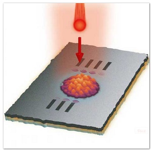
In a breakthrough for future optical-electronic hybrid computers, scientists at EPFL have developed an ultrafast technique that can track light and electrons as they travel through a nanostructured surface.
An illustration of the experimental set-up described in this study. (Image: F. Carbone/EPFL)
When light couples to electrons on a surface, their concerted motion can travel as a wave guided by the surface geometry itself. These waves are known as "surface plasmons" and might be useful in telecommunications and future computing, where data will be shuttled across processors using light instead of electricity. Aside from being more energy-efficient, these processors could be miniaturized down to the nanoscale to build high-resolution sensors and nanosized signal processing systems. But these processors would be built from stacking different layers of advanced materials and, so far, we don't have a reliable way of tracking the guided light as it moves across their interfaces.
EPFL scientists have now done exactly that using a new, ultrafast method. The breakthrough is published today in Nature Communications ("Imaging and controlling plasmonic interference fields at buried interfaces").
The lab of Fabrizio Carbone at EPFL led the project to create a tiny antenna array that would allow plasmons to travel across an interface. The array consisted of an extremely thin membrane of silicon nitride (50 nm thick) covered with an even thinner film of silver (30 nm thick). The scientists then "punched" a series of nano-holes through the surface that would act as the antennas -- the plasmon "hotspots".
The researchers then fired ultrafast laser pulses (light) onto the array to light up the antennas. With a controlled temporal delay, ultrashort electron pulses were then fired across the multilayer stack, to map the plasmons radiated by the antennas at the interface between the silver film and the silicon nitride membrane. Using an ultrafast technique called PINEM, which can "see" surface plasmons, even when they are bound to a buried interface, the scientists were able to actually film the propagation of the guided light and read its spatial profile across the film.
"Trying to see plasmons in these interfaces between layers is a bit like trying to film people in a house from the outside," explains Fabrizio Carbone. "A regular camera won't show you anything; but if you use microwave or a similar energy-tracking imaging, you can see right through the walls."
The current paper paves the way for designing and controlling confined plasmonic fields in multilayered structures, which is key for future optoelectronic devices.
Share on:


Suggested Items
Real Time with… IPC APEX EXPO 2024: Exploring the Future of Surface Finishes
04/25/2024 | Real Time with...IPC APEX EXPOJoe McGurran, product marketing director for MKS Atotech, looks into the future of surface finishes, discussing less nickel, reduced thickness, technologies influencing HDI and UHDI, and the benefits of nickel-free surface finishes. He also touches on popular finishes like ENIG and palladium immersion gold and discusses the value proposition of making a change.
Designer’s Notebook: What Designers Need to Know About Manufacturing, Part 2
04/24/2024 | Vern Solberg -- Column: Designer's NotebookThe printed circuit board (PCB) is the primary base element for providing the interconnect platform for mounting and electrically joining electronic components. When assessing PCB design complexity, first consider the component area and board area ratio. If the surface area for the component interface is restricted, it may justify adopting multilayer or multilayer sequential buildup (SBU) PCB fabrication to enable a more efficient sub-surface circuit interconnect.
IDTechEx Report Unveils 3D Electronics Status and Opportunities
04/22/2024 | PRNewswire3D electronics is an emerging manufacturing approach that enables electronics to be integrated within or onto the surface of objects. 3D electronic manufacturing techniques empower new features, including mass customizability, greater integration, and improved sustainability in the electronics industry.
NASA, Japan Advance Space Cooperation, Sign Agreement for Lunar Rover
04/11/2024 | NASANASA Administrator Bill Nelson and Japan’s Minister of Education, Culture, Sports, Science and Technology (MEXT) Masahito Moriyama have signed an agreement to advance sustainable human exploration of the Moon.
Lockheed Martin Conducts Historic LRASM Flight Test
04/04/2024 | Lockheed MartinThe U.S. Navy in partnership with Lockheed Martin [NYSE: LMT] successfully conducted a historic Long-Range Anti-Ship Missile (LRASM) flight test with four missiles simultaneously in flight.