


 It’s Only Common Sense: Nice Guys Really Can Finish First
 The Right Approach: I Hear the Train A Comin'
 Marcy's Musings: The Growing Industry
Engineers Reveal Fabrication Process for Revolutionary Transparent Sensors
October 14, 2016 | University of Wisconsin-MadisonEstimated reading time: 1 minute
In 2014, when University of Wisconsin-Madison engineers announced in the journal Nature Communications ("Graphene-based carbon-layered electrode array technology for neural imaging and optogenetic applications") that they had developed transparent sensors for use in imaging the brain, researchers around the world took notice.
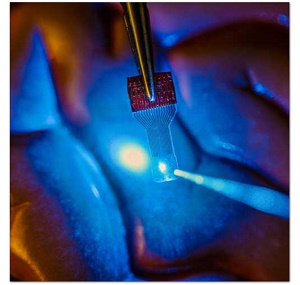
A blue light shines through a clear, implantable medical sensor onto a brain model. See-through sensors, which have been developed by a team of UW–Madison engineers, should help neural researchers better view brain activity. (Image: Justin Williams research group)
Then the requests came flooding in. "So many research groups started asking us for these devices that we couldn't keep up," says Zhenqiang (Jack) Ma, the Lynn H. Matthias Professor and Vilas Distinguished Achievement Professor in electrical and computer engineering at UW-Madison.
Ma's group is a world leader in developing revolutionary flexible electronic devices. The see-through, implantable micro-electrode arrays were light years beyond anything ever created.
Although he and collaborator Justin Williams, the Vilas Distinguished Achievement Professor in biomedical engineering and neurological surgery at UW-Madison, patented the technology through the Wisconsin Alumni Research Foundation, they saw its potential for advancements in research. "That little step has already resulted in an explosion of research in this field," says Williams. "We didn't want to keep this technology in our lab. We wanted to share it and expand the boundaries of its applications."
As a result, in a paper published Thursday in the journal Nature Protocols ("Fabrication and utility of a transparent graphene neural electrode array for electrophysiology, in vivo imaging, and optogenetics"), the researchers have described in great detail how to fabricate and use transparent graphene neural electrode arrays in applications in electrophysiology, fluorescent microscopy, optical coherence tomography, and optogenetics. "We described how to do these things so we can start working on the next generation," says Ma.
Now, not only are the UW-Madison researchers looking at ways to improve and build upon the technology, they also are seeking to expand its applications from neuroscience into areas such as research of stroke, epilepsy, Parkinson's disease, cardiac conditions, and many others. And they hope other researchers do the same.
"This paper is a gateway for other groups to explore the huge potential from here," says Ma. "Our technology demonstrates one of the key in vivo applications of graphene. We expect more revolutionary research will follow in this interdisciplinary field."
Share on:


Suggested Items
Samsung Electronics Begins Industry’s First Mass Production of 9th-Gen V-NAND
04/29/2024 | Samsung ElectronicsSamsung Electronics, the world leader in advanced memory technology, today announced that it has begun mass production for its one-terabit (Tb) triple-level cell (TLC) 9th-generation vertical NAND (V-NAND), solidifying its leadership in the NAND flash market.
TSMC Celebrates 30th North America Technology Symposium
04/29/2024 | TSMCTSMC unveiled its newest semiconductor process, advanced packaging, and 3D IC technologies for powering the next generation of AI innovations with silicon leadership at the Company’s 2024 North America Technology Symposium.
QinetiQ Achieves UK’s First Jet-to-Jet Teaming Between Aircraft and Autonomous Drone
04/29/2024 | QinetiQQinetiQ has successfully trialled the UK’s first Crewed-Uncrewed-Teaming demonstration between a crewed aircraft and an autonomous jet drone.
Warm Windows and Streamlined Skin Patches – IDTechEx Explores Flexible and Printed Electronics
04/26/2024 | IDTechExFlexible and printed electronics can be integrated into cars and homes to create modern aesthetics that are beneficial and easy to use. From luminous car controls to food labels that communicate the quality of food, the uses of this technology are endless and can upgrade many areas of everyday life.
iNEMI Packaging Tech Topic Series: Role of EDA in Advanced Semiconductor Packaging
04/26/2024 | iNEMIAdvanced semiconductor packaging with heterogenous integration has made on-package integration of multiple chips a crucial part of finding alternatives to transistor scaling. Historically, EDA tools for front-end and back-end design have evolved separately; however, design complexity and the increased number of die-to-die or die-to-substrate interconnections has led to the need for EDA tools that can support integration of overall design planning, implementation, and system analysis in a single cockpit.