


 It’s Only Common Sense: Nice Guys Really Can Finish First
 The Right Approach: I Hear the Train A Comin'
 Marcy's Musings: The Growing Industry
iPhone 7: Apple Underwent Strategic Change by Selecting TSMC’s inFO Platform
October 21, 2016 | Yole DéveloppementEstimated reading time: 2 minutes
Each year, Apple integrates more and more innovative technologies in its iPhone products. This year, with the new iPhone 7 and its A10 processor, the leading company is the first organization to bring out PoP WLP at the consumer scale. Apple underwent a strategic change by selecting TSMC’s new inFO-PoP packaging technology for its new A10 processor. Without doubt, this technical choice had a strong impact on the advanced packaging industry: according to Yole Développement (Yole), fan-out activity revenues forecast should reach about US$ 2.5 billion in 2021, with 80% growth between 2015 and 2017.
System Plus Consulting, proposes today a detailed technology analysis of Apple’s A10 processor, named TSMC Integrated Fan-Out (inFO) Package in Apple’s A10 Application Processor. Under this report, the reverse engineering and costing company provides a comprehensive understanding of the A10 manufacturing processes as well as accurate estimations of manufacturing costs and selling prices. With more than 100 relevant technical and strategic analyses per year, System Plus Consulting analysts combine their technical, marketing, reverse engineering and costing know-how in the “More than Moore” semiconductor industry, to be at the cutting edge of innovation and the most recent technologies and provide deep added-value analysis.
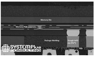
IPhone 7 & A10 application processor: what’s inside?
Located on the main board, A10 application processor (bottom package) and the DRAM Chip (top package) have been developed in a PoP configuration. Depending on the version, iPhone 7 or iPhone 7 Plus, the DRAM memory has different space management. Apple’s A10 is a wafer-level package using TSMC’s packaging technology with copper pillar Through inFO Vias. This technology is replacing the well-known Through Molded Via approach. “With this new technology, Apple has made a huge break from traditional PoP packaging found in previous AP generations”, asserts Stéphane Elisabeth, RF and Advanced Packaging Cost Engineer at System Plus Consulting.
In this report, System Plus Consulting highlights Apple’s latest innovations at the packaging level. Indeed the company is offering an in-depth analysis of the package process including copper pillars, redistribution layer, and silicon high density capacitor integration. The deep trench capacitor is the first integrated component developed by TSMC for high-volume consumer applications. System Plus Consulting had also available a detail report on this capacitor.
A detailed comparison has been performed by System Plus Consulting’s experts and especially the pros and cons of inFO technology compared to PoP packaging selected by Samsung for its Exynos 8 processor and by Qualcomm for the development of its Snapdragon 820 processor (for Samsung as well).
Thanks to the inFO process, Apple is able today to offer a very thin package on package, with a high number of I/O pads and better thermal management. According to System Plus Consulting’s report, the A10 processor is showing an impressive thickness reduction of 30% compared to traditional PoP-based systems. In addition, TSMC removed a lot of expensive manufacturing steps. “The result is a very cost-effective component that can compete with any well-known PoP” comments Stéphane Elisabeth from System Plus Consulting.
The new reverse engineering and costing report from System Plus Consulting compares costs with other chips and includes a technical comparison with the previous Apple AP, the A9.
Share on:


Suggested Items
Designer’s Notebook: What Designers Need to Know About Manufacturing, Part 2
04/24/2024 | Vern Solberg -- Column: Designer's NotebookThe printed circuit board (PCB) is the primary base element for providing the interconnect platform for mounting and electrically joining electronic components. When assessing PCB design complexity, first consider the component area and board area ratio. If the surface area for the component interface is restricted, it may justify adopting multilayer or multilayer sequential buildup (SBU) PCB fabrication to enable a more efficient sub-surface circuit interconnect.
Insulectro’s 'Storekeepers' Extend Their Welcome to Technology Village at IPC APEX EXPO
04/03/2024 | InsulectroInsulectro, the largest distributor of materials for use in the manufacture of PCBs and printed electronics, welcomes attendees to its TECHNOLOGY VILLAGE during this year’s IPC APEX EXPO at the Anaheim Convention Center, April 9-11, 2024.
ENNOVI Introduces a New Flexible Circuit Production Process for Low Voltage Connectivity in EV Battery Cell Contacting Systems
04/03/2024 | PRNewswireENNOVI, a mobility electrification solutions partner, introduces a more advanced and sustainable way of producing flexible circuits for low voltage signals in electric vehicle (EV) battery cell contacting systems.
Heavy Copper PCBs: Bridging the Gap Between Design and Fabrication, Part 1
04/01/2024 | Yash Sutariya, Saturn Electronics ServicesThey call me Sparky. This is due to my talent for getting shocked by a variety of voltages and because I cannot seem to keep my hands out of power control cabinets. While I do not have the time to throw the knife switch to the off position, that doesn’t stop me from sticking screwdrivers into the fuse boxes. In all honesty, I’m lucky to be alive. Fortunately, I also have a talent for building high-voltage heavy copper circuit boards. Since this is where I spend most of my time, I can guide you through some potential design for manufacturability (DFM) hazards you may encounter with heavy copper design.
Trouble in Your Tank: Supporting IC Substrates and Advanced Packaging, Part 5
03/19/2024 | Michael Carano -- Column: Trouble in Your TankDirect metallization systems based on conductive graphite or carbon dispersion are quickly gaining acceptance worldwide. Indeed, the environmental and productivity gains one can achieve with these processes are outstanding. In today’s highly competitive and litigious environment, direct metallization reduces costs associated with compliance, waste treatment, and legal issues related to chemical exposure. What makes these processes leaders in the direct metallization space?