


 The Chemical Connection: Reducing Etch System Water Usage, Part 2
 It’s Only Common Sense: Nice Guys Really Can Finish First
 The Right Approach: I Hear the Train A Comin'
Electrons in Graphene Behave Like Light, Only Better
October 25, 2016 | Columbia UniversityEstimated reading time: 6 minutes
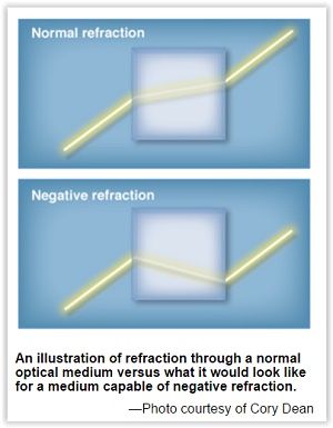
A team led by Cory Dean, assistant professor of physics at Columbia University, Avik Ghosh, professor of electrical and computer engineering at the University of Virginia, and James Hone, Wang Fong-Jen Professor of Mechanical Engineering at Columbia Engineering, has directly observed—for the first time—negative refraction for electrons passing across a boundary between two regions in a conducting material. First predicted in 2007, this effect has been difficult to confirm experimentally. The researchers were able to observe the effect in graphene, demonstrating that electrons in the atomically thin material behave like light rays, which can be manipulated by such optical devices as lenses and prisms. The findings, which are published in the September 30 edition of Science, could lead to the development of new types of electron switches, based on the principles of optics rather than electronics.
“The ability to manipulate electrons in a conducting material like light rays opens up entirely new ways of thinking about electronics,” says Dean. “For example, the switches that make up computer chips operate by turning the entire device on or off, and this consumes significant power. Using lensing to steer an electron ‘beam’ between electrodes could be dramatically more efficient, solving one of the critical bottlenecks to achieving faster and more energy efficient electronics.”
Dean adds, “These findings could also enable new experimental probes. For example, electron lensing could enable on-chip versions of an electron microscope, with the ability to perform atomic scale imaging and diagnostics. Other components inspired by optics, such as beam splitters and interferometers, could additionally enable new studies of the quantum nature of electrons in the solid state.”
While graphene has been widely explored for supporting high electron speed, it is notoriously hard to turn off the electrons without hurting their mobility. Ghosh says, “The natural follow-up is to see if we can achieve a strong current turn-off in graphene with multiple angled junctions. If that works to our satisfaction, we’ll have on our hands a low-power, ultra-high-speed switching device for both analog (RF) and digital (CMOS) electronics, potentially mitigating many of the challenges we face with the high energy cost and thermal budget of present day electronics.”
Light changes direction – or refracts - when passing from one material to another, a process that allows us to use lenses and prisms to focus and steer light. A quantity known as the index of refraction determines the degree of bending at the boundary, and is positive for conventional materials such as glass. However, through clever engineering, it is also possible to create optical “metamaterials” with a negative index, in which the angle of refraction is also negative. “This can have unusual and dramatic consequences,” Hone notes. “Optical metamaterials are enabling exotic and important new technologies such as super lenses, which can focus beyond the diffraction limit, and optical cloaks, which make objects invisible by bending light around them.”
Electrons travelling through very pure conductors can travel in straight lines like light rays, enabling optics-like phenomena to emerge. In materials, the electron density plays a similar role to the index of refraction, and electrons refract when they pass from a region of one density to another. Moreover, current carriers in materials can either behave like they are negatively charged (electrons) or positively charged (holes), depending on whether they inhabit the conduction or the valence band. In fact, boundaries between hole-type and electron-type conductors, known as p-n junctions (“p” positive, “n” negative), form the building blocks of electrical devices such as diodes and transistors.
“Unlike in optical materials”, says Hone, “where creating a negative index metamaterial is a significant engineering challenge, negative electron refraction occurs naturally in solid state materials at any p-n junction.”
The development of two-dimensional conducting layers in high-purity semiconductors such as GaAs (Gallium arsenide) in the 1980s and 1990s allowed researchers to first demonstrate electron optics including the effects of both refraction and lensing. However, in these materials, electrons travel without scattering only at very low temperatures, limiting technological applications. Furthermore, the presence of an energy gap between the conduction and valence band scatters electrons at interfaces and prevents observation of negative refraction in semiconductor p-n junctions. In this study, the researchers’ use of graphene, a 2D material with unsurpassed performance at room temperature and no energy gap, overcame both of these limitations.
The possibility of negative refraction at graphene p-n junctions was first proposed in 2007 by theorists working at both the University of Lancaster and Columbia University. However, observation of this effect requires extremely clean devices, such that the electrons can travel ballistically, without scattering, over long distances. Over the past decade, a multidisciplinary team at Columbia - including Hone and Dean, along with Kenneth Shepard, Lau Family Professor of Electrical Engineering and professor of biomedical engineering, Abhay Pasupathy, associate professor of physics, and Philip Kim, professor of physic at the time (now at Harvard) – has worked to develop new techniques to construct extremely clean graphene devices. This effort culminated in the 2013 demonstration of ballistic transport over a length scale in excess of 20 microns. Since then, they have been attempting to develop a Veselago lens, which focuses electrons to a single point using negative refraction. But they were unable to observe such an effect and found their results puzzling.
In 2015, a group at Pohang University of Science and Technology in South Korea reported the first evidence focusing in a Veselago-type device. However, the response was weak, appearing in the signal derivative. The Columbia team decided that to fully understand why the effect was so elusive, they needed to isolate and map the flow of electrons across the junction. They utilized a well-developed technique called “magnetic focusing” to inject electrons onto the p-n junction. By measuring transmission between electrodes on opposite sides of the junction as a function of carrier density they could map the trajectory of electrons on both sides of the p-n junction as the incident angle was changed by tuning the magnetic field.
Crucial to the Columbia effort was the theoretical support provided by Ghosh’s group at the University of Virginia, who developed detailed simulation techniques to model the Columbia team’s measured response. This involved calculating the flow of electrons in graphene under the various electric and magnetic fields, accounting for multiple bounces at edges, and quantum mechanical tunneling at the junction. The theoretical analysis also shed light on why it has been so difficult to measure the predicted Veselago lensing in a robust way, and the group is developing new multi-junction device architectures based on this study. Together the experimental data and theoretical simulation gave the researchers a visual map of the refraction, and enabled them to be the first to quantitatively confirm the relationship between the incident and refracted angles (known as Snell’s Law in optics), as well as confirmation of the magnitude of the transmitted intensity as a function of angle (known as the Fresnel coefficients in optics).
“In many ways, this intensity of transmission is a more crucial parameter,” says Ghosh, “since it determines the probability that electrons actually make it past the barrier, rather than just their refracted angles. The transmission ultimately determines many of the performance metrics for devices based on these effects, such as the on-off ratio in a switch, for example.”
The Science study was supported by Semiconductor Research Corporation’s NRI Center for Institute for Nanoelectronics Discovery and Exploration (INDEX). The collaboration was made possible through the support of the NRI program, which has brought together some of the country’s best groups in the study of 2D materials to focus on novel device architectures that may outperform conventional silicon-based technologies.
Share on:


Suggested Items
Indium Corporation Expert to Present on Pb-Free Solder for Die-Attach in Discrete Power Applications
04/30/2024 | Indium CorporationIndium Corporation Product Manager – Semiconductor Dean Payne will present at the Advanced Packaging for Power Electronics conference, hosted by IMAPS, held May 8-9 in Woburn, Massachusetts, USA.
Boeing Opens Research & Technology Center in Japan
04/23/2024 | BoeingBoeing today opened a Boeing Research & Technology (BR&T) Center in Japan that will focus on innovation to enable the commercial aviation industry meet its goal of net zero carbon emissions by 2050.
Ansys Joins BAE Systems’ Mission Advantage Program to Advance Digital Engineering Across US Department of Defense
04/16/2024 | ANSYSAnsys announced it is working with BAE Systems, Inc., to accelerate the adoption of digital engineering and MBSE across the Department of Defense (DoD).
Incap Estonia Teamed Up With Solaride to Fuel Youth Excitement for The World of Engineering
04/11/2024 | IncapIncap Estonia partnered with Solaride to ignite enthusiasm among young people for the world of engineering and sustainable technology. Together, they organised an inspiring day for students from grades 7 through 12 in Saaremaa. Held at Incap’s Kuressaare factory, this event brought together over 130 young minds eager to explore the innovative world of technology and learn more about advanced electronics manufacturing.
Mark Schulman Rocks Zuken Innovation World + integrate24
04/10/2024 | ZukenZuken USA, Inc. is excited to announce that the renowned drummer and motivational speaker, Mark Schulman, will be the keynote speaker at this year's Zuken Innovation World Americas (ZIW) conference, co-located with integrate24. Scheduled for September 17-19, 2024, in the vibrant city of Cleveland, Ohio, the conference aims to bring together the brightest minds in the PCB, Wire Harness, and Digital Engineering fields.