


 The Chemical Connection: Reducing Etch System Water Usage, Part 2
 It’s Only Common Sense: Nice Guys Really Can Finish First
 The Right Approach: I Hear the Train A Comin'
On-chip Observation of THz Graphene Plasmons
November 7, 2016 | Elhuyar FundazioaEstimated reading time: 2 minutes
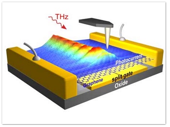
Researchers developed a technique for imaging THz photocurrents with nanoscale resolution, and applied it to visualize strongly compressed THz waves (plasmons) in a graphene photodetector. The extremely short wavelengths and highly concentrated fields of these plasmons open new venues for the development of miniaturized optoelectronic THz devices.
THz photocurrent nanoscopy of graphene plasmons in a split-gate photodetector
Radiation in the terahertz (THz) frequency range is attracting large interest because of its manifold application potential for non-destructive imaging, next-generation wireless communication or sensing. But still, the generating, detecting and controlling of THz radiation faces numerous technological challenges. Particularly, the relatively long wavelengths (from 30 to 300 mm) of THz radiation require solutions for nanoscale integration of THz devices or for nanoscale sensing and imaging applications.
In recent years, graphene plasmonics has become a highly promising platform for shrinking THz waves. It is based on the interaction of light with collective electron oscillations in graphene, giving rise to electromagnetic waves that are called plasmons. The graphene plasmons propagate with strongly reduced wavelength and can concentrate THz fields to subwavelength-scale dimensions, while the plasmons themselves can be controlled electrically.
Now, researchers at CIC nanoGUNE (San Sebastian, Spain) in collaboration with ICFO (Barcelona, Spain), IIT (Genova, Italy) - members of the EU Graphene Flagship - Columbia University (New York, USA), Radboud University (Nijmegen, Netherlands), NIM (Tsukuba, Japan) and Neaspec (Martinsried, Germany) could visualize strongly compressed and confined THz plasmons in a room-temperature THz detector based on graphene. To see the plasmons, they recorded a nanoscale map of the photocurrent that the detector produced while a sharp metal tip was scanned across it. The tip had the function to focus the THz illumination to a spot size of about 50 nm, which is about 2000 times smaller than the illumination wavelength. This new imaging technique, named THz photocurrent nanoscopy, provides unprecedented possibilities for characterizing optoelectronic properties at THz frequencies.
The team recorded photocurrent images of the graphene detector, while it was illuminated with THz radiation of around 100 mm wavelength. The images showed photocurrent oscillations revealing that THz plasmons with a more than 50 times reduced wavelength were propagating in the device while producing a photocurrent.
“In the beginning we were quite surprised about the extremely short plasmon wavelength, as THz graphene plasmons are typically much less compressed”, says former nanoGUNE researcher Pablo Alonso, now at the University of Oviedo, and first author of the work. “We managed to solve the puzzle by theoretical studies, which showed that the plasmons couple with the metal gate below the graphene”, he continues. “This coupling leads to an additional compression of the plasmons and an extreme field confinement, which could open the door towards various detector and sensor applications”, adds Rainer Hillenbrand, Ikerbasque Research Professor and Nanooptics Group Leader at nanoGUNE who led the research. The plasmons also show a linear dispersion – that means that their energy is proportional to their momentum - which could be beneficial for information and communication technologies. The team also analysed the lifetime of the THz plasmons, which showed that the damping of THz plasmons is determined by the impurities in the graphene.
THz photocurrent nanoscopy relies on the strong photothermoelectric effect in graphene, which transforms heat generated by THz fields, including that of THz plasmons, into a current. In the future, the strong thermoelectric effect could be also applied for on-chip THz plasmon detection in graphene plasmonic circuits. The technique for THz photocurrent nanoimaging could find further application potential beyond plasmon imaging, for example, for studying the local THz optoelectronic properties of other 2D materials, classical 2D electron gases or semiconductor nanostructures.
Share on:


Suggested Items
Real Time with… IPC APEX EXPO 2024: Direct Imaging Equipment and Quad-wave DLP Light Engine Technology
05/03/2024 | Real Time with...IPC APEX EXPOGuest Editor Kelly Dack and MivaTek's Brendan Hogan delve into the company's innovative technologies, including direct imaging equipment and quad-wave DLP light engine technology. They highlight the benefits of direct imaging, compensation, and DART technology.
Merlin Flex invests in New Schmoll Direct Imaging System
04/30/2024 | Merlin Flex LtdMerlin Flex has fully installed and commissioned its 2nd Schmoll MDI Direct Imaging system. This new machine includes a twin bed, 4 head system which enhances Merlin Flex’s direct imaging capability for its 1.4M long flexible circuits.
Inkjet Solder Mask ‘Has Arrived’
04/10/2024 | Pete Starkey, I-Connect007I was delighted to be invited to attend an interactive webinar entitled “Solder Mask Coating Made Easy with Additive Manufacturing,” hosted by SUSS MicroTec Netherlands in Eindhoven. The webinar was introduced and moderated by André Bodegom, managing director at Adeon Technologies, and the speakers were Mariana Van Dam, senior product manager PCB imaging solutions at AGFA in Belgium; Ashley Steers, sales manager at Electra Polymers in the UK; and Dr. Luca Gautero, product manager at SUSS MicroTec Netherlands.
NetVia Group Acquires Direct Imaging from Mivatek
04/09/2024 | Miva TechnologiesMiva Technologies is pleased to announce NetVia Group, Irving, TX has acquired a new Miva 2400NG Dual Tray Direct Imaging System with 30-micron capabilities for inner, outer and soldermask imaging.
Teledyne to Acquire Adimec
02/13/2024 | TeledyneTeledyne Technologies Incorporated announced that it has entered into an agreement to acquire Adimec Holding B.V. and its subsidiaries.