


 The Right Approach: I Hear the Train A Comin'
 It’s Only Common Sense: OCCAM—the Time Is Now
 Marcy's Musings: The Growing Industry
Biomedical 'Skin-like Bandage' is Stretchy, Durable and Long Lasting
November 16, 2016 | Purdue UniversityEstimated reading time: 2 minutes
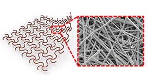
A skin-like biomedical technology that uses a mesh of conducting nanowires and a thin layer of elastic polymer might bring new electronic bandages that monitor biosignals for medical applications and provide therapeutic stimulation through the skin.
The biomedical device mimics the human skin's elastic properties and sensory capabilities.
"It can intimately adhere to the skin and simultaneously provide medically useful biofeedback such as electrophysiological signals," said Chi Hwan Lee, an assistant professor of biomedical engineering and mechanical engineering at Purdue University. "Uniquely, this work combines high-quality nanomaterials into a skin-like device, thereby enhancing the mechanical properties."
The device could be likened to an electronic bandage and might be used to treat medical conditions using thermotherapeutics, where heat is applied to promote vascular flow for enhanced healing, said Lee, who worked with a team that includes Purdue graduate student Min Ku Kim.
Traditional approaches to developing such a technology have used thin films made of ductile metals such as gold, silver and copper.
A skin-like biomedical technology that uses a mesh of conducting nanowires and a thin layer of elastic polymer might bring new "electronic bandages." (Purdue University image/Min Ku Kim) Download image
"The problem is that these thin films are susceptible to fractures by over-stretching and cracking," Lee said. "Instead of thin films we use nanowire mesh film, which makes the device more resistive to stretching and cracking than otherwise possible. In addition, the nanowire mesh film has very high surface area compared to conventional thin films, with more than 1,000 times greater surface roughness. So once you attach it to the skin the adhesion is much higher, reducing the potential of inadvertent delamination."
"Recording the electrophysiological signals from the skin can provide wearers and clinicians with quantitative measures of the heart's activity or the muscle's activity," Lee said.
Much of the research was performed in the Birck Nanotechnology Center in Purdue's Discovery Park.
"The nanowires mesh film was initially formed on a conventional silicon wafer with existing micro- and nano-fabrication technologies. Our unique technique, called a crack-driven transfer printing technique, allows us to controllably peel off the device layer from the silicon wafer, and then apply onto the skin," Lee said.
The Oklahoma State researchers contributed theoretical simulations related to the underlying mechanics of the devices, and Seungyong Han synthesized and provided the conducting nanowires.
Future research will be dedicated to developing a transdermal drug-delivery bandage that would transport medications through the skin in an electronically controlled fashion. Such a system might include built-in sensors to detect the level of injury and autonomously deliver the appropriate dose of drugs.
Share on:


Suggested Items
Designer’s Notebook: What Designers Need to Know About Manufacturing, Part 2
04/24/2024 | Vern Solberg -- Column: Designer's NotebookThe printed circuit board (PCB) is the primary base element for providing the interconnect platform for mounting and electrically joining electronic components. When assessing PCB design complexity, first consider the component area and board area ratio. If the surface area for the component interface is restricted, it may justify adopting multilayer or multilayer sequential buildup (SBU) PCB fabrication to enable a more efficient sub-surface circuit interconnect.
Insulectro’s 'Storekeepers' Extend Their Welcome to Technology Village at IPC APEX EXPO
04/03/2024 | InsulectroInsulectro, the largest distributor of materials for use in the manufacture of PCBs and printed electronics, welcomes attendees to its TECHNOLOGY VILLAGE during this year’s IPC APEX EXPO at the Anaheim Convention Center, April 9-11, 2024.
ENNOVI Introduces a New Flexible Circuit Production Process for Low Voltage Connectivity in EV Battery Cell Contacting Systems
04/03/2024 | PRNewswireENNOVI, a mobility electrification solutions partner, introduces a more advanced and sustainable way of producing flexible circuits for low voltage signals in electric vehicle (EV) battery cell contacting systems.
Heavy Copper PCBs: Bridging the Gap Between Design and Fabrication, Part 1
04/01/2024 | Yash Sutariya, Saturn Electronics ServicesThey call me Sparky. This is due to my talent for getting shocked by a variety of voltages and because I cannot seem to keep my hands out of power control cabinets. While I do not have the time to throw the knife switch to the off position, that doesn’t stop me from sticking screwdrivers into the fuse boxes. In all honesty, I’m lucky to be alive. Fortunately, I also have a talent for building high-voltage heavy copper circuit boards. Since this is where I spend most of my time, I can guide you through some potential design for manufacturability (DFM) hazards you may encounter with heavy copper design.
Trouble in Your Tank: Supporting IC Substrates and Advanced Packaging, Part 5
03/19/2024 | Michael Carano -- Column: Trouble in Your TankDirect metallization systems based on conductive graphite or carbon dispersion are quickly gaining acceptance worldwide. Indeed, the environmental and productivity gains one can achieve with these processes are outstanding. In today’s highly competitive and litigious environment, direct metallization reduces costs associated with compliance, waste treatment, and legal issues related to chemical exposure. What makes these processes leaders in the direct metallization space?