


 The Right Approach: I Hear the Train A Comin'
 It’s Only Common Sense: OCCAM—the Time Is Now
 Marcy's Musings: The Growing Industry
Designer Materials Create Miniature Computer Circuits
November 22, 2016 | University of ManchesterEstimated reading time: 1 minute
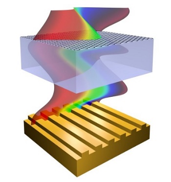
Scientists at The University of Manchester have discovered a new method of creating optoelectronic circuits using graphene and other 2D materials that are much smaller than their current counterparts.
Optoelectronics, the technology that uses pulses of light rather than traditional electrical signals, is vital for telecommunication networks.
Modulators are important in optoelectronic circuits as they control the signals passed through optoelectronic devices. Previous attempts to create hybrid modulators incorporating graphene have yielded promising although limited results.
Writing in Nature Communications, researchers led by Professor Sasha Grigorenko have shown it is possible to combine graphene, its sister material boron nitride and a nanoscale gold grating to create a new class of optical modulator.
Graphene is the world’s first two-dimensional material, just one atom thick yet 200 times stronger than steel, more conductive than copper and impermeable to water.
Since then a whole family of 2D materials have been uncovered and are now being used together in order to tailor materials to meet specific requirements.
The proposed device can effectively process information using light much the same way as computers process information using electrons.
Graphene NOWNANO PhD student Philip Thomas, who led the experimental work, said: “This could pave the way for faster circuits, which is the main selling point of using light instead of electrical signals. But probably the bigger result from this work is that it could allow for a dramatic reduction in the size of these circuits. It is rare to have a modulator which both creates a strong modulation effect and is really tiny.”
Professor Sasha Grigorenko said: “It is unprecedented to achieve light modulation in such a wide wavelength range - from visible to infrared light in which human eye, night vision goggles and thermal imaging operate - using just one simple design.”
Share on:


Suggested Items
Designer’s Notebook: What Designers Need to Know About Manufacturing, Part 2
04/24/2024 | Vern Solberg -- Column: Designer's NotebookThe printed circuit board (PCB) is the primary base element for providing the interconnect platform for mounting and electrically joining electronic components. When assessing PCB design complexity, first consider the component area and board area ratio. If the surface area for the component interface is restricted, it may justify adopting multilayer or multilayer sequential buildup (SBU) PCB fabrication to enable a more efficient sub-surface circuit interconnect.
Insulectro’s 'Storekeepers' Extend Their Welcome to Technology Village at IPC APEX EXPO
04/03/2024 | InsulectroInsulectro, the largest distributor of materials for use in the manufacture of PCBs and printed electronics, welcomes attendees to its TECHNOLOGY VILLAGE during this year’s IPC APEX EXPO at the Anaheim Convention Center, April 9-11, 2024.
ENNOVI Introduces a New Flexible Circuit Production Process for Low Voltage Connectivity in EV Battery Cell Contacting Systems
04/03/2024 | PRNewswireENNOVI, a mobility electrification solutions partner, introduces a more advanced and sustainable way of producing flexible circuits for low voltage signals in electric vehicle (EV) battery cell contacting systems.
Heavy Copper PCBs: Bridging the Gap Between Design and Fabrication, Part 1
04/01/2024 | Yash Sutariya, Saturn Electronics ServicesThey call me Sparky. This is due to my talent for getting shocked by a variety of voltages and because I cannot seem to keep my hands out of power control cabinets. While I do not have the time to throw the knife switch to the off position, that doesn’t stop me from sticking screwdrivers into the fuse boxes. In all honesty, I’m lucky to be alive. Fortunately, I also have a talent for building high-voltage heavy copper circuit boards. Since this is where I spend most of my time, I can guide you through some potential design for manufacturability (DFM) hazards you may encounter with heavy copper design.
Trouble in Your Tank: Supporting IC Substrates and Advanced Packaging, Part 5
03/19/2024 | Michael Carano -- Column: Trouble in Your TankDirect metallization systems based on conductive graphite or carbon dispersion are quickly gaining acceptance worldwide. Indeed, the environmental and productivity gains one can achieve with these processes are outstanding. In today’s highly competitive and litigious environment, direct metallization reduces costs associated with compliance, waste treatment, and legal issues related to chemical exposure. What makes these processes leaders in the direct metallization space?