


 The Right Approach: I Hear the Train A Comin'
 It’s Only Common Sense: OCCAM—the Time Is Now
 Marcy's Musings: The Growing Industry
Supersonic Spray Yields New Nanomaterial for Bendable, Wearable Electronics
November 23, 2016 | University of Illinois at ChicagoEstimated reading time: 2 minutes
A new, ultrathin film that is both transparent and highly conductive to electric current has been produced by a cheap and simple method devised by an international team of nanomaterials researchers from the University of Illinois at Chicago and Korea University.
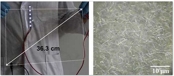
Left, photograph of a large-scale silver nanowire-coated flexible film. Right, silver nanowire particles viewed under the microscope
The film is also bendable and stretchable, offering potential applications in roll-up touchscreen displays, wearable electronics, flexible solar cells and electronic skin. The results are reported in Advanced Functional Materials ("Production of Flexible Transparent Conducting Films of Self-Fused Nanowires via One-Step Supersonic Spraying").
Left, photograph of a large-scale silver nanowire-coated flexible film. Right, silver nanowire particles viewed under the microscope. (Image: S.K. Yoon, Korea University) (click on image to enlarge)
The new film is made of fused silver nanowires, and is produced by spraying the nanowire particles through a tiny jet nozzle at supersonic speed. The result is a film with nearly the electrical conductivity of silver-plate -- and the transparency of glass, says senior author Alexander Yarin, UIC Distinguished Professor of Mechanical Engineering.
"The silver nanowire is a particle, but very long and thin," Yarin said. The nanowires measure about 20 microns long, so four laid end-to-end would span the width of a human hair. But their diameter is a thousand times smaller -- and significantly smaller than the wavelength of visible light, which minimizes light scattering.
The researchers suspended the nanowire particles in water and propelled them by air through a de Laval nozzle, which has the same geometry as a jet engine, but is only a few millimeters in diameter.
"The liquid needs to be atomized so it evaporates in flight," Yarin said. When the nanowires strike the surface they are being applied to at supersonic speed, they fuse together, as their kinetic energy is converted to heat.
"The ideal speed is 400 meters per second," Yarin said. "If the energy is too high, say 600 meters per second, it cuts the wires. If too low, as at 200 meters per second, there's not enough heat to fuse the wires."
The researchers applied the nanowires to flexible plastic films and to three-dimensional objects. "The surface shape doesn't matter," Yarin said.
The transparent flexible film can be bent repeatedly and stretched to seven times its original length and still work, said Sam Yoon, the corresponding author of the study and a professor of mechanical engineering at Korea University.
Earlier this year, Yarin and Yoon and their colleagues produced a transparent conducting film by electroplating a mat of tangled nanofiber with copper. Compared to that film, the self-fused silver nanowire film offers better scalability and production rate, Yoon said.
"It should be easier and cheaper to fabricate, as it's a one-step versus a two-step process," said Yarin. "You can do it roll-to-roll on an industrial line, continuously."
Share on:


Suggested Items
Designer’s Notebook: What Designers Need to Know About Manufacturing, Part 2
04/24/2024 | Vern Solberg -- Column: Designer's NotebookThe printed circuit board (PCB) is the primary base element for providing the interconnect platform for mounting and electrically joining electronic components. When assessing PCB design complexity, first consider the component area and board area ratio. If the surface area for the component interface is restricted, it may justify adopting multilayer or multilayer sequential buildup (SBU) PCB fabrication to enable a more efficient sub-surface circuit interconnect.
Insulectro’s 'Storekeepers' Extend Their Welcome to Technology Village at IPC APEX EXPO
04/03/2024 | InsulectroInsulectro, the largest distributor of materials for use in the manufacture of PCBs and printed electronics, welcomes attendees to its TECHNOLOGY VILLAGE during this year’s IPC APEX EXPO at the Anaheim Convention Center, April 9-11, 2024.
ENNOVI Introduces a New Flexible Circuit Production Process for Low Voltage Connectivity in EV Battery Cell Contacting Systems
04/03/2024 | PRNewswireENNOVI, a mobility electrification solutions partner, introduces a more advanced and sustainable way of producing flexible circuits for low voltage signals in electric vehicle (EV) battery cell contacting systems.
Heavy Copper PCBs: Bridging the Gap Between Design and Fabrication, Part 1
04/01/2024 | Yash Sutariya, Saturn Electronics ServicesThey call me Sparky. This is due to my talent for getting shocked by a variety of voltages and because I cannot seem to keep my hands out of power control cabinets. While I do not have the time to throw the knife switch to the off position, that doesn’t stop me from sticking screwdrivers into the fuse boxes. In all honesty, I’m lucky to be alive. Fortunately, I also have a talent for building high-voltage heavy copper circuit boards. Since this is where I spend most of my time, I can guide you through some potential design for manufacturability (DFM) hazards you may encounter with heavy copper design.
Trouble in Your Tank: Supporting IC Substrates and Advanced Packaging, Part 5
03/19/2024 | Michael Carano -- Column: Trouble in Your TankDirect metallization systems based on conductive graphite or carbon dispersion are quickly gaining acceptance worldwide. Indeed, the environmental and productivity gains one can achieve with these processes are outstanding. In today’s highly competitive and litigious environment, direct metallization reduces costs associated with compliance, waste treatment, and legal issues related to chemical exposure. What makes these processes leaders in the direct metallization space?