


 The Right Approach: I Hear the Train A Comin'
 It’s Only Common Sense: OCCAM—the Time Is Now
 Marcy's Musings: The Growing Industry
Squeezing Light Into New Miniature Devices
November 28, 2016 | Institute for Basic ScienceEstimated reading time: 2 minutes
Do you think your computer is fast enough? Think again. The computers of the future could work almost at the speed of light! Nanophotonics, the study of light at the nanometer scale, could indeed bring the speed of our technology to a completely different level.
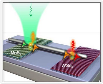
The multiplexer device with one input and two outputs. The plus-minus couple indicates the exciton.
The Center for Integrated Nanostructure Physics (CINAP) within the Institute for Basic Science (IBS) have developed three key components of a circuit that works with light. Published in Nature Communications ("Reconfigurable exciton-plasmon interconversion for nanophotonic circuits"), these devices combine the advantages of photonics and electronics on the same platform.
While we are slowing approaching the end point of Moore's Law: a state where we physically cannot shrink the dimension of our transistors much further; the future of big data processing requires high performance computers with higher speed operations. Researchers reckon that if we build computers that process information through light, instead of electrons, computer will be able to work faster.
However, at nanometer dimensions, the wavelength of light is larger than the diameter of the silicon fiber and for this reason some light can be lost. A solution to control the propagation of light in matter can come from surface plasmons. These are electromagnetic waves that propagate along the surface of some conductive materials like silver, gold, aluminum and copper. Using surface plasmons, optical information can be transmitted nearly at the speed of light and in extremely miniature volumes.
Using surface plasmons in silver nanowires and 2D semiconductors like molybdenum disulphide (MoS2), IBS scientists built three key components for optical communication: optical transistors, optical multiplexers and optical signal detectors.
These devices work thanks to a phenomenon called plasmon-exciton-plasmon interconversion. The graphics describe the details of this process step-by-step.
IBS scientists constructed the optical transistor by interconnecting the silver nanowire to a flake of MoS2. Light shone on the device is converted to surface plasmon, than to exciton, back to surface plasmon and eventually emitted as light with a shorter wavelength compared to the initial input. For example, if the input light is green, the output light can be red.
Wavelength multiplexing devices were realized in a similar way, but instead of having only a flake of MoS2, the researchers used an array of three different 2D semiconductor materials emitting light at different wavelengths. In this structure, for example, a single input light (violet color) generates three output lights (blue, green and red).
The propagating optical signals along the silver nanowire can be also transformed and detected as electrical signals by an optical signal detector.
“The originality of this paper arises from the exciton-plasmon interconversion. We published before the conversion of exciton to plasmon, and from plasmon to exciton using silver nanowire/2D semiconductor hybrids, but this is the first time that we can complete the circle going from plasmons to excitons and back to plasmons. Using this concept, we created optical transistors and multiplexors,” explains professor Hyun Seok Lee, first author of this study.
Share on:


Suggested Items
Designer’s Notebook: What Designers Need to Know About Manufacturing, Part 2
04/24/2024 | Vern Solberg -- Column: Designer's NotebookThe printed circuit board (PCB) is the primary base element for providing the interconnect platform for mounting and electrically joining electronic components. When assessing PCB design complexity, first consider the component area and board area ratio. If the surface area for the component interface is restricted, it may justify adopting multilayer or multilayer sequential buildup (SBU) PCB fabrication to enable a more efficient sub-surface circuit interconnect.
Insulectro’s 'Storekeepers' Extend Their Welcome to Technology Village at IPC APEX EXPO
04/03/2024 | InsulectroInsulectro, the largest distributor of materials for use in the manufacture of PCBs and printed electronics, welcomes attendees to its TECHNOLOGY VILLAGE during this year’s IPC APEX EXPO at the Anaheim Convention Center, April 9-11, 2024.
ENNOVI Introduces a New Flexible Circuit Production Process for Low Voltage Connectivity in EV Battery Cell Contacting Systems
04/03/2024 | PRNewswireENNOVI, a mobility electrification solutions partner, introduces a more advanced and sustainable way of producing flexible circuits for low voltage signals in electric vehicle (EV) battery cell contacting systems.
Heavy Copper PCBs: Bridging the Gap Between Design and Fabrication, Part 1
04/01/2024 | Yash Sutariya, Saturn Electronics ServicesThey call me Sparky. This is due to my talent for getting shocked by a variety of voltages and because I cannot seem to keep my hands out of power control cabinets. While I do not have the time to throw the knife switch to the off position, that doesn’t stop me from sticking screwdrivers into the fuse boxes. In all honesty, I’m lucky to be alive. Fortunately, I also have a talent for building high-voltage heavy copper circuit boards. Since this is where I spend most of my time, I can guide you through some potential design for manufacturability (DFM) hazards you may encounter with heavy copper design.
Trouble in Your Tank: Supporting IC Substrates and Advanced Packaging, Part 5
03/19/2024 | Michael Carano -- Column: Trouble in Your TankDirect metallization systems based on conductive graphite or carbon dispersion are quickly gaining acceptance worldwide. Indeed, the environmental and productivity gains one can achieve with these processes are outstanding. In today’s highly competitive and litigious environment, direct metallization reduces costs associated with compliance, waste treatment, and legal issues related to chemical exposure. What makes these processes leaders in the direct metallization space?