


 The Right Approach: I Hear the Train A Comin'
 It’s Only Common Sense: OCCAM—the Time Is Now
 Marcy's Musings: The Growing Industry
Researchers Explore New 2D Materials That Could Make Devices Faster, Smaller, and Efficient
November 29, 2016 | University of Minnesota College of Science and EngineeringEstimated reading time: 2 minutes
A new study by an international team of researchers led by the University of Minnesota highlights how manipulation of 2D materials could make our modern day devices faster, smaller, and better.
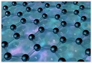
Two-dimensional materials are a class of nanomaterials that are only a few atoms in thickness. Electrons in these materials are free to move in the two-dimensional plane, but their restricted motion in the third direction is governed by quantum mechanics. Research on these nanomaterials is still in its infancy, but 2D materials such as graphene, transition metal dichalcogenides and black phosphorus have garnered tremendous attention from scientists and engineers for their amazing properties and potential to improve electronic and photonic devices.
In this study, researchers from the University of Minnesota, MIT, Stanford, U.S. Naval Research Laboratory, IBM, and universities in Brazil, UK and Spain, teamed up to examine the optical properties of several dozens of 2D materials. The goal of the paper is to unify understanding of light-matter interactions in these materials among researchers and explore new possibilities for future research.
They discuss how polaritons, a class of quasiparticles formed through the coupling of photons with electric charge dipoles in solid, allow researchers to marry the speed of photon light particles and the small size of electrons.
“With our devices, we want speed, efficiency, and we want small. Polaritons could offer the answer,” said Tony Low, a University of Minnesota electrical and computer engineering assistant professor and lead author of the study.
By exciting the polaritons in 2D materials, electromagnetic energy can be focused down to a volume a million times smaller compared to when its propagating in free space.
“Layered two-dimensional materials have emerged as a fantastic toolbox for nano-photonics and nano-optoelectronics, providing tailored design and tunability for properties that are not possible to realize with conventional materials,” said Frank Koppens, group leader at the Institute of Photonic Sciences at Barcelona, Spain, and co-author of the study. “This will offer tremendous opportunities for applications.”
Others on the team from private industry also recognize the potential in practical applications.
“The study of the plasmon-polaritons in two-dimensions is not only a fascinating research subject, but also offers possibilities for important technological applications,” said Phaedon Avoruris, IBM Fellow at the IBM T. J. Watson Research Center and co-author of the study. “For example, an atomic layer material like graphene extends the field of plasmonics to the infrared and terahertz regions of the electromagnetic spectrum allowing unique applications ranging from sensing and fingerprinting minute amounts of biomolecules, to applications in optical communications, energy harvesting and security imaging.”
The new study also examined the possibilities of combining 2D materials. Researchers point out that every 2D material has advantages and disadvantages. Combining these materials create new materials that may have the best qualities of both.
“Every time we look at a new material, we find something new,” Low said. “Graphene is often considered a ‘wonder’ material, but combining it with another material may make it even better for a wide variety of applications.”
In addition to Low, Avoruris and Koppens, other researchers involved in the study include Andrey Chaves, Universidade Federal do Cearán (Brazil) and Columbia University; Joshua D. Caldwell, U.S. Naval Research Laboratory; Anshuman Kumar, University of Minnesota and Massachusetts Institute of Technology; Nicholas X.Fang, MIT; Tony Heinz, Stanford University; Francisco Guinea, IMDEA Nanociencia and University of Manchester; and Luis Martin-Moreno, University of Zaragoza (Spain).
Share on:


Suggested Items
Real Time with... IPC APEX EXPO 2024: Sustainability in the Industry
04/26/2024 | Real Time with...IPC APEX EXPOGuest Editor Henry Crandall and Chris Nash of Indium Corporation discuss the company's 90th anniversary and its focus on sustainability. They focus on the benefits of sustainable materials, their compatibility, and value propositions. The conversation also highlights how Durafuse LT technology's role in reducing reflow temperatures is leading to significant cost and energy savings. Nash also touches on downstream sustainability efforts such as using recycled materials for packaging.
SMC Korea 2024 to Highlight Semiconductor Materials Trends and Innovations on Industry’s Path to $1 Trillion
04/24/2024 | SEMIWith Korea a major consumer of semiconductor materials and advanced materials a key driver of innovation on the industry’s path to $1 trillion, industry leaders and experts will gather at SMC (Strategic Materials Conference) Korea 2024 on May 29 at the Suwon Convention Center in Gyeonggi-do, South Korea to provide insights into the latest materials developments and trends. Registration is open.
Groundbreaking Ceremony Marks the Beginning of a New Era for Newccess Industrial; The Construction of the MINGXIN Building
04/12/2024 | Newccess IndustrialOn a clear and sunny day in March, the groundbreaking ceremony for the MINGXIN Building took place in Shenzhen, China. This moment marked the official commencement of construction for a project that will reshape the semiconductor materials industry.
The Need for a Holistic Global Sustainability Standard
04/10/2024 | Michael Ford, Aegis SoftwareNo one can deny that the resources of our fragile planet are finite. The environment seems like a third party, subject to constant degradation. We’re acutely aware of the effects of pollution on our climate, and despite our “throw-away” culture, recycling and recovery of materials has remained relatively expensive, even as we use more energy just to survive.
iNEMI Publishes Four Roadmap Topics
04/04/2024 | iNEMIThe International Electronics Manufacturing Initiative (iNEMI) announces the availability of the first roadmap topics in the new iNEMI Roadmap format. Printed circuit boards, sustainable electronics, smart manufacturing, and mmWave materials and test are now available online.