


 The Right Approach: I Hear the Train A Comin'
 It’s Only Common Sense: OCCAM—the Time Is Now
 Marcy's Musings: The Growing Industry
Graphene Calligraphy
December 8, 2016 | University of ManchesterEstimated reading time: 2 minutes
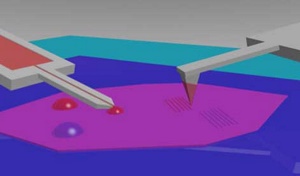
Scientists at The University of Manchester and Karlsruhe Institute of Technology have demonstrated a method to chemically modify small regions of graphene with high precision, leading to extreme miniaturisation of chemical and biological sensors.
Writing in ACS Applied Materials & Interfaces ("Attoliter Chemistry for Nanoscale Functionalization of Graphene"), researchers led by Dr. Aravind Vijayaraghavan have shown that it is possible to combine graphene with chemical and biological molecules and form patterns, which are 100s of nanometres wide.
Graphene is the world’s first two-dimensional material. It is strong, transparent, flexible and the world’s most conductive material. Every atom in graphene is exposed to its environment, allowing it to sense changes in its surroundings.
Using technology that resembles writing with a quill or fountain pen, the scientists were able to deliver chemical droplets to the surface of graphene in very small volumes. In order to achieve such fine chemical patterns, the researchers used droplets of chemicals less than 100 attolitres (10-16 L) in volume; that’s 1/10,000,000,000,000,000th of a litre.
Two types of ‘pens’ were used, one which is dipped into the reactive ‘ink’ like a quill to cover the nib, and the other where the ink is filled into a reservoir and flows through a channel in the nib, just like in a fountain pen. An array of such micro-pens are moved over the graphene surface to deliver the chemical droplets which react with the graphene.
These techniques are key to enabling graphene sensors which can be used in real-world applications; graphene sensors fabricated this way have the potential to be used in blood tests, minimising the amount of blood a patient is required to give.
Dr. Vijayaraghavan explains: “Two types of ‘pens’ were used, one which is dipped into the reactive ‘ink’ like a quill to cover the nib, and the other where the ink is filled into a reservoir and flows through a channel in the nib, just like in a fountain pen. An array of such micro-pens are moved over the graphene surface to deliver the chemical droplets which react with the graphene. The first method is known as Dip-Pen Nanolithography (DPN) and the latter is known as Microchannel Cantilever Spotting (µCS).”
Dr. Michael Hirtz, co-investigator from Karlsruhe adds: “By chemically modifying the graphene in such small regions, we can develop chemical and biological sensors which only require very small volumes of fluid to detect various constituents. This, combined with the high sensitivity of graphene sensors, leads us to imagine that in the future we could perform a full blood test on a patient with just one tiny drop of blood, instead of a full syringe.”
Share on:


Suggested Items
D Coupon Testing and Data Insights With GreenSource Fabrication
04/17/2024 | Marcy LaRont, PCB007 MagazineMarcy LaRont spoke with Steve Karas of GreenSource Fabrication at the SMTA UHDI conference in March. He presented a case study that GreenSource undertook with a customer on critical via reliability with advanced materials and used the experience to highlight the importance and effectiveness of D coupon testing. He also discussed GreenSource’s approach to data aggregation and a new system they developed to use collected data effectively.
IPC Publishes Comprehensive Strategy to Address Electronics Industry’s Global Workforce Challenge
04/10/2024 | IPCOne of the most difficult and urgent challenges facing the electronics industry is a chronic shortage of adequately skilled workers. Today, IPC unveiled an expansion of its strategy to address the workforce challenges of the U.S. electronics manufacturing industry and called on its more than 3,000 member companies to join in the effort.
UHDI Fundamentals: ASC Sponsors Ultra High Density Interconnect Symposium
03/21/2024 | Anaya Vardya, American Standard CircuitsAmerican Standard Circuits (ASC) is a major sponsor of an upcoming symposium on one of the most talked about new technologies that has come along in quite a while: ultra high density interconnect (UHDI).
onsemi Aligns Business Groups to Expand Product Portfolio and Accelerate Growth
03/13/2024 | onsemionsemi announced the formation of the Analog and Mixed-Signal Group (AMG) which will be led by newly appointed group president, Sudhir Gopalswamy.
Indium Corporation Experts to Present at SEMI THERM
03/07/2024 | Indium CorporationIndium Corporation Global Account Manager and Senior Thermal Technologist Tim Jensen and Product Development Specialist for Thermal Interface Materials Miloš Lazić will present on thermal interface material (TIM) technology at SEMI-THERM, taking place March 25–28 in San Jose, California, U.S.