


 It’s Only Common Sense: Nice Guys Really Can Finish First
 The Right Approach: I Hear the Train A Comin'
 Marcy's Musings: The Growing Industry
Germanium's Semiconducting and Optical Properties Probed Under Pressure
January 4, 2017 | Carnegie Institution for ScienceEstimated reading time: 2 minutes
Germanium may not be a household name like silicon, its group-mate on the periodic table, but it has great potential for use in next-generation electronics and energy technology.
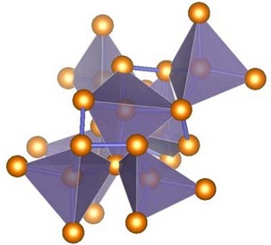
This is an illustration of ST12-germanium's complex tetragonal structure with tetrahedral bonding. (Image: Haidong Zhang)
Of particular interest are forms of germanium that can be synthesized in the lab under extreme pressure conditions. However, one of the most-promising forms of germanium for practical applications, called ST12, has only been created in tiny sample sizes--too small to definitively confirm its properties.
"Attempts to experimentally or theoretically pin down ST12-germanium's characteristics produced extremely varied results, especially in terms of its electrical conductivity," said Carnegie's Zhisheng Zhao, the first author on a new paper about this form of germanium.
The study's research team, led by Carnegie's Timothy Strobel, was able to create ST12-germanium in a large enough sample size to confirm its characteristics and useful properties. Their work is published by Nature Communications ("Properties of the exotic metastable ST12 germanium allotrope").
"This work will be of interest to a broad range of readers in the field of materials science, physics, chemistry, and engineering," explained Carnegie's Haidong Zhang, the co-leading author.
ST12-germanium has a tetragonal structure--the nameST12 means "simple tetragonal with 12 atoms." It was created by putting germanium under about 138 times normal atmospheric pressure (14 gigapascals) and then decompressing it slowly at room temperature.
The millimeter-sized samples of ST12-germanium that the team created were large enough that they could be studied using a variety of spectroscopic techniques in order to confirm its long-debated characteristics.
Like the most common, diamond-cubic form of germanium, they found that ST12 is a semiconductor with a so-called indirect band gap. Metallic substances conduct electrical current easily, whereas insulating materials conduct no current at all. Semiconducting materials exhibit mid-range electrical conductivity. When semiconducting materials are subjected to an input of a specific energy, bound electrons can be moved to higher-energy, conducting states. The specific energy required to make this jump to the conducting state is defined as the "band gap." While direct band gap materials can effectively absorb and emit light, indirect band gap materials cannot.
"Our team was able to quantify ST12's optical band gap--where visible light energy can be absorbed by the material--as well as its electrical and thermal properties, which will help define its potential for practical applications," Strobel said. "Our findings indicate that due to the size of its band gap, ST12-germanium may be a better material for infrared detection and imaging technology than the diamond-cubic form of the element already being used for these purposes."
Share on:


Suggested Items
Real Time with... IPC APEX EXPO 2024: Sustainability in the Industry
04/26/2024 | Real Time with...IPC APEX EXPOGuest Editor Henry Crandall and Chris Nash of Indium Corporation discuss the company's 90th anniversary and its focus on sustainability. They focus on the benefits of sustainable materials, their compatibility, and value propositions. The conversation also highlights how Durafuse LT technology's role in reducing reflow temperatures is leading to significant cost and energy savings. Nash also touches on downstream sustainability efforts such as using recycled materials for packaging.
SMC Korea 2024 to Highlight Semiconductor Materials Trends and Innovations on Industry’s Path to $1 Trillion
04/24/2024 | SEMIWith Korea a major consumer of semiconductor materials and advanced materials a key driver of innovation on the industry’s path to $1 trillion, industry leaders and experts will gather at SMC (Strategic Materials Conference) Korea 2024 on May 29 at the Suwon Convention Center in Gyeonggi-do, South Korea to provide insights into the latest materials developments and trends. Registration is open.
Groundbreaking Ceremony Marks the Beginning of a New Era for Newccess Industrial; The Construction of the MINGXIN Building
04/12/2024 | Newccess IndustrialOn a clear and sunny day in March, the groundbreaking ceremony for the MINGXIN Building took place in Shenzhen, China. This moment marked the official commencement of construction for a project that will reshape the semiconductor materials industry.
The Need for a Holistic Global Sustainability Standard
04/10/2024 | Michael Ford, Aegis SoftwareNo one can deny that the resources of our fragile planet are finite. The environment seems like a third party, subject to constant degradation. We’re acutely aware of the effects of pollution on our climate, and despite our “throw-away” culture, recycling and recovery of materials has remained relatively expensive, even as we use more energy just to survive.
iNEMI Publishes Four Roadmap Topics
04/04/2024 | iNEMIThe International Electronics Manufacturing Initiative (iNEMI) announces the availability of the first roadmap topics in the new iNEMI Roadmap format. Printed circuit boards, sustainable electronics, smart manufacturing, and mmWave materials and test are now available online.