


 It’s Only Common Sense: Would You Join Your Own Company?
 The Chemical Connection: Reducing Etch System Water Usage, Part 2
 The Right Approach: I Hear the Train A Comin'
Researchers Directly Measure How Perovskite Solar Films Efficiently Convert Light to Power
January 12, 2017 | Case Western Reserve UniversityEstimated reading time: 3 minutes
Solar cells made with films mimicking the structure of the mineral perovskite are the focus of worldwide research. But only now have researchers at Case Western Reserve University directly shown the films bear a key property allowing them to efficiently convert sunlight into electricity.
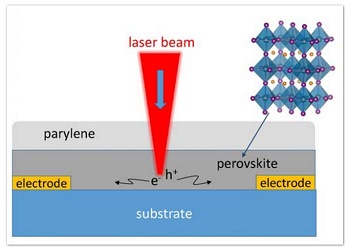
This is a schematic of scanning photocurrent imaging microscopy of halide perovskite film (side view). Using the technique, researchers found the diffusion length within a well-oriented perovskite film measured up to 20 micrometers.
Identifying that attribute could lead to more efficient solar panels.
Electrons generated when light strikes the film are unrestricted by grain boundaries -- the edges of crystalline subunits within the film -- and travel long distances without deteriorating, the researchers showed. That means electric charge carriers that become trapped and decay in other materials are instead available to be drawn off as current.
The scientists directly measured the distance traveled--called diffusion length -- for the first time by using the technique called "spatially scanned photocurrent imaging microscopy." Diffusion length within a well-oriented perovskite film measured up to 20 micrometers.
The findings, published in the journal Nano Letters ("Imaging the Long Transport Lengths of Photo-generated Carriers in Oriented Perovskite Films"), indicate that solar cells could be made thicker without harming their efficiency, said Xuan Gao, associate professor of physics and author of the paper.
"A thicker cell can absorb more light," he said, "potentially yielding a better solar cell."
Efficiency built in
Solar power researchers believe perovskite films hold great promise. In less than five years, films made with the crystalline structure have surpassed 20 percent efficiency in converting sunlight to electricity, a mark that took decades to reach with silicon-based solar cells used today.
In this research, Gao's lab performed spatially scanned photocurrent image measurements on films made in the lab of Case Western Reserve chemistry professor Clemens Burda.
Perovskite minerals found in nature are oxides of certain metals, but Burda's lab made organo-metallic films with the same crystalline structure using methyl ammonium lead tri-iodide (CH3NH3PBI3), a three-dimensional lead halide surrounded by small organic methyl ammonium molecules that hold the lattice structure together.
"The question has been, 'How are these solar cells so efficient? If we would know, we could further improve perovskite solar cells" Burda said. "People thought it could be due to unusually long electron transport, and we directly measured it."
Diffusion length is the distance an electron or its opposite, called a hole, travels from generation until it recombines or is extracted as electric current. The distance is the same as transport length when no electric field (which usually increases the distance traveled) is applied.
Measuring travel
The labs made repeated measurements by focusing a tiny laser spot on films 8 millimeters square by 300 nanometers thick. The films were made stable by coating the perovskite with a layer of the polymer parylene.
The light generates electrons and holes and the photocurrent, or stream of electrons, is recorded between the electrodes positioned about 120 microns away from each other while the film is scanned along two perpendicular directions. The scanning yields a two-dimensional spatial map of carrier diffusion and transport characteristics.
The measurements showed diffusion length averaged about 10 microns. In some cases, the length reached 20 microns, showing the functional area of the film is at least 20 microns long, the researchers said.
In some materials, grain boundaries decrease conductivity, but imaging showed that these interfaces between grains in the film exerted no influence on electron travel. Gao and Burda say this may be because grains in the film are well aligned, causing no impedance or other detrimental effects on electrons or holes.
Burda and Gao are now seeking federal funds to use the microscopy technique to determine whether different grain sizes, orientations, halide perovskite compositions, film thicknesses and more change the film's properties, to further accelerate research in the field.
Share on:


Suggested Items
Real Time with… IPC APEX EXPO 2024: Direct Imaging Equipment and Quad-wave DLP Light Engine Technology
05/03/2024 | Real Time with...IPC APEX EXPOGuest Editor Kelly Dack and MivaTek's Brendan Hogan delve into the company's innovative technologies, including direct imaging equipment and quad-wave DLP light engine technology. They highlight the benefits of direct imaging, compensation, and DART technology.
Merlin Flex invests in New Schmoll Direct Imaging System
04/30/2024 | Merlin Flex LtdMerlin Flex has fully installed and commissioned its 2nd Schmoll MDI Direct Imaging system. This new machine includes a twin bed, 4 head system which enhances Merlin Flex’s direct imaging capability for its 1.4M long flexible circuits.
Inkjet Solder Mask ‘Has Arrived’
04/10/2024 | Pete Starkey, I-Connect007I was delighted to be invited to attend an interactive webinar entitled “Solder Mask Coating Made Easy with Additive Manufacturing,” hosted by SUSS MicroTec Netherlands in Eindhoven. The webinar was introduced and moderated by André Bodegom, managing director at Adeon Technologies, and the speakers were Mariana Van Dam, senior product manager PCB imaging solutions at AGFA in Belgium; Ashley Steers, sales manager at Electra Polymers in the UK; and Dr. Luca Gautero, product manager at SUSS MicroTec Netherlands.
NetVia Group Acquires Direct Imaging from Mivatek
04/09/2024 | Miva TechnologiesMiva Technologies is pleased to announce NetVia Group, Irving, TX has acquired a new Miva 2400NG Dual Tray Direct Imaging System with 30-micron capabilities for inner, outer and soldermask imaging.
Teledyne to Acquire Adimec
02/13/2024 | TeledyneTeledyne Technologies Incorporated announced that it has entered into an agreement to acquire Adimec Holding B.V. and its subsidiaries.