


 It’s Only Common Sense: Nice Guys Really Can Finish First
 The Right Approach: I Hear the Train A Comin'
 Marcy's Musings: The Growing Industry
Sustainable Manufacturing
January 26, 2017 | University of UtahEstimated reading time: 1 minute
Rochester Institute of Technology’s Golisano Institute for Sustainability (GIS) was selected this week by the U.S. Department of Energy, as part of its Manufacturing USA initiative, to lead its new Reducing Embodied-Energy and Decreasing Emissions (REMADE) Institute — a national coalition of leading universities and companies that will forge new clean energy initiatives deemed critical in keeping U.S. manufacturing competitive.
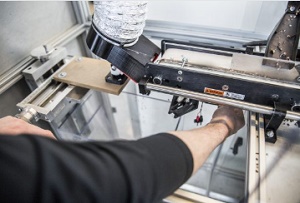
The University of Utah has been actively involved in developing new metal and material recycling technologies. Professor Rajamani’s research group has invented a new technology to sort aluminum and copper from recycled automobile scrap. PHOTO CREDIT: Dave Titensor/University of Utah
The REMADE Institute, under the RIT-led Sustainable Manufacturing Innovation Alliance (SMIA), will leverage up to $70 million in federal funding that will be matched by $70 million in private cost-share commitments from industry and other consortium members, including 85 partners.
The institute will focus its efforts on driving down the cost of technologies essential to reuse, recycle and remanufacture materials such as metals, fibers, polymers and electronic waste and aims to achieve a 50% improvement in overall energy efficiency by 2027. These efficiency measures could save billions of dollars in energy costs and improve U.S. economic competitiveness through innovative new manufacturing techniques, small business opportunities and offer new training and jobs for American workers.
The Department of Metallurgical Engineering, the College of Mines and Earth Sciences, the Global Change and Sustainability Center, and other entities at the University of Utah will work in collaboration with Idaho National Lab, Argonne National Lab, University of Illinois and other leading universities, national labs and industrial partners in partnership with the U.S. Department of Energy. In all, 26 universities, 44 companies, seven national labs, 26 industry trade associations and foundations and three states (New York, Colorado and Utah) are engaged in the effort.
Economic impact and workforce development
REMADE Institute partners have the following five-year goals:
- 5% to 10% improvement in manufacturing material efficiency by reducing manufacturing material waste
- 50% increase in remanufacturing applications
- 30% increase in efficiency of remanufacturing operations
- 30% increase in recycling efficiencies
- A targeted 50 percent increase in sales for the U.S. manufacturing industry to $21.5 billion and the creation of a next-generation recycling and manufacturing workforce.
The REMADE Institute also will develop and implement an education and workforce development program that will fill workforce gaps identified by its industry, government and academic partners and build the next generation of the recycling and remanufacturing workforce.
Share on:


Suggested Items
Designer’s Notebook: What Designers Need to Know About Manufacturing, Part 2
04/24/2024 | Vern Solberg -- Column: Designer's NotebookThe printed circuit board (PCB) is the primary base element for providing the interconnect platform for mounting and electrically joining electronic components. When assessing PCB design complexity, first consider the component area and board area ratio. If the surface area for the component interface is restricted, it may justify adopting multilayer or multilayer sequential buildup (SBU) PCB fabrication to enable a more efficient sub-surface circuit interconnect.
Insulectro’s 'Storekeepers' Extend Their Welcome to Technology Village at IPC APEX EXPO
04/03/2024 | InsulectroInsulectro, the largest distributor of materials for use in the manufacture of PCBs and printed electronics, welcomes attendees to its TECHNOLOGY VILLAGE during this year’s IPC APEX EXPO at the Anaheim Convention Center, April 9-11, 2024.
ENNOVI Introduces a New Flexible Circuit Production Process for Low Voltage Connectivity in EV Battery Cell Contacting Systems
04/03/2024 | PRNewswireENNOVI, a mobility electrification solutions partner, introduces a more advanced and sustainable way of producing flexible circuits for low voltage signals in electric vehicle (EV) battery cell contacting systems.
Heavy Copper PCBs: Bridging the Gap Between Design and Fabrication, Part 1
04/01/2024 | Yash Sutariya, Saturn Electronics ServicesThey call me Sparky. This is due to my talent for getting shocked by a variety of voltages and because I cannot seem to keep my hands out of power control cabinets. While I do not have the time to throw the knife switch to the off position, that doesn’t stop me from sticking screwdrivers into the fuse boxes. In all honesty, I’m lucky to be alive. Fortunately, I also have a talent for building high-voltage heavy copper circuit boards. Since this is where I spend most of my time, I can guide you through some potential design for manufacturability (DFM) hazards you may encounter with heavy copper design.
Trouble in Your Tank: Supporting IC Substrates and Advanced Packaging, Part 5
03/19/2024 | Michael Carano -- Column: Trouble in Your TankDirect metallization systems based on conductive graphite or carbon dispersion are quickly gaining acceptance worldwide. Indeed, the environmental and productivity gains one can achieve with these processes are outstanding. In today’s highly competitive and litigious environment, direct metallization reduces costs associated with compliance, waste treatment, and legal issues related to chemical exposure. What makes these processes leaders in the direct metallization space?