


 It’s Only Common Sense: Nice Guys Really Can Finish First
 The Right Approach: I Hear the Train A Comin'
 Marcy's Musings: The Growing Industry
Polycrystalline Materials in Solar Cells Gain New Impulse With Findings From INL Researchers
January 30, 2017 | INLEstimated reading time: 1 minute
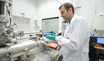
The conversion of sunlight into electricity through solar cells is considered to be a future cornerstone in a renewable energy supply for a sustainable society. The semiconducting compound Cu(In,Ga)Se2, which is deposited as a thin polycrystalline layer onto a metallized glass carrier, has long been known as an excellent light absorber. In the last 5 years, the power conversion efficiency of solar cells based on this material has reached new record values, from ~19.8% in 2011 to 22.6% in 2016, within reach of those of the commercially dominating silicon wafer technology. These recent advances have been achieved through the introduction of a potassium-fluoride treatment of the Cu(In,Ga)Se2 material. It is generally assumed that this treatment mainly affects the region of and near the charge-separating interface.
Researchers of the International Iberian Nanotechnology Laboratory (INL) in Braga have now demonstrated that also the electronic properties of the grain boundaries between the grains of the light absorbing layer are beneficially affected by the potassium treatment.
The study was performed in collaboration with researchers from the Institut des Matériaux Jean Rouxel (IMN) from the University of Nantes, who fabricated the solar cell samples and was published today in Scientific Reports, Effect of the KF post-deposition treatment on grain boundary properties in Cu(In, Ga)Se2 thin films an open access journal published by the Nature Group.
The researchers used an advanced scanning probe microscopy method to image electronic surface properties with nanometer-scale spatial resolution. “We were able to show that the potassium treatment results in a stronger and more homogeneous electronic effect at the grain boundaries” says Nicoleta Nicoara, member of the Laboratory of Nanostructured Solar Cells at INL involved in the research. Polycrystalline semiconductor materials can usually be fabricated more cost-efficient at lower processing temperatures compared to single-crystalline materials. However, the presence of grain boundaries limits their use in many applications, as they lead to losses in performance due to the presence of defects. Sascha Sadewasser who led this study summarizes: “Our study demonstrates that the potassium fluoride treatment can beneficially modify the properties of grain boundaries in Cu(In,Ga)Se2 solar cell materials. The insight we gained through our study might well influence research directions in other polycrystalline materials, and animate researcher to search for treatments with similarly positive effects on the electronic properties of grain boundaries”.
Share on:


Suggested Items
Real Time with... IPC APEX EXPO 2024: Sustainability in the Industry
04/26/2024 | Real Time with...IPC APEX EXPOGuest Editor Henry Crandall and Chris Nash of Indium Corporation discuss the company's 90th anniversary and its focus on sustainability. They focus on the benefits of sustainable materials, their compatibility, and value propositions. The conversation also highlights how Durafuse LT technology's role in reducing reflow temperatures is leading to significant cost and energy savings. Nash also touches on downstream sustainability efforts such as using recycled materials for packaging.
SMC Korea 2024 to Highlight Semiconductor Materials Trends and Innovations on Industry’s Path to $1 Trillion
04/24/2024 | SEMIWith Korea a major consumer of semiconductor materials and advanced materials a key driver of innovation on the industry’s path to $1 trillion, industry leaders and experts will gather at SMC (Strategic Materials Conference) Korea 2024 on May 29 at the Suwon Convention Center in Gyeonggi-do, South Korea to provide insights into the latest materials developments and trends. Registration is open.
Groundbreaking Ceremony Marks the Beginning of a New Era for Newccess Industrial; The Construction of the MINGXIN Building
04/12/2024 | Newccess IndustrialOn a clear and sunny day in March, the groundbreaking ceremony for the MINGXIN Building took place in Shenzhen, China. This moment marked the official commencement of construction for a project that will reshape the semiconductor materials industry.
The Need for a Holistic Global Sustainability Standard
04/10/2024 | Michael Ford, Aegis SoftwareNo one can deny that the resources of our fragile planet are finite. The environment seems like a third party, subject to constant degradation. We’re acutely aware of the effects of pollution on our climate, and despite our “throw-away” culture, recycling and recovery of materials has remained relatively expensive, even as we use more energy just to survive.
iNEMI Publishes Four Roadmap Topics
04/04/2024 | iNEMIThe International Electronics Manufacturing Initiative (iNEMI) announces the availability of the first roadmap topics in the new iNEMI Roadmap format. Printed circuit boards, sustainable electronics, smart manufacturing, and mmWave materials and test are now available online.