


 It’s Only Common Sense: Nice Guys Really Can Finish First
 The Right Approach: I Hear the Train A Comin'
 Marcy's Musings: The Growing Industry
Absorbing Electromagnetic Energy While Avoiding the Heat
January 30, 2017 | Duke UniversityEstimated reading time: 2 minutes
Electrical engineers at Duke University have created the world's first electromagnetic metamaterial made without any metal. The device's ability to absorb electromagnetic energy without heating up has direct applications in imaging, sensing and lighting.
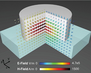
A closer look at one of the cylinders comprising a new non-metal metamaterial. The arrows depict how different aspects of an electromagnetic field interact with the cylinder.
Metamaterials are synthetic materials composed of many individual, engineered features that together produce properties not found in nature. Imagine an electromagnetic wave moving through a flat surface made of thousands of tiny electrical cells. If researchers can tune each cell to manipulate the wave in a specific way, they can dictate exactly how the wave behaves as a whole.
For researchers to manipulate electromagnetic waves, however, they've typically had to use electrically conducting metals. That approach, however, brings with it a fundamental problem of metals—the higher the electrical conductivity, the better the material also conducts heat. This limits their usefulness in temperature-dependent applications.
In a new paper, electrical engineers at Duke University demonstrate the first completely dielectric (non-metal) electromagnetic metamaterial—a surface dimpled with cylinders like the face of a Lego brick that is designed to absorb terahertz waves. While this specific frequency range sits between infrared waves and microwaves, the approach should be applicable for almost any frequency of the electromagnetic spectrum.
The results appeared online on Jan. 9 in the journal Optics Express.
"People have created these types of devices before, but previous attempts with dielectrics have always been paired with at least some metal," said Willie Padilla, professor of electrical and computer engineering at Duke University. "We still need to optimize the technology, but the path forward to several applications is much easier than with metal-based approaches."
Padilla and his colleagues created their metamaterial with boron-doped silicon—a non-metal. Using computer simulations, they calculated how terahertz waves would interact with cylinders of varying heights and widths.
The researchers then manufactured a prototype consisting of hundreds of these optimized cylinders aligned in rows on a flat surface. Physical tests showed that the new "metasurface" absorbed 97.5 percent of the energy produced by waves at 1.011 terahertz.
Efficiently absorbing energy from electromagnetic waves is an important property for many applications. For example, thermal imaging devices can operate in the terahertz range, but because they have previously included at least some metal, getting sharp images has been challenging.
"Heat propagates fast in metals, which is problematic for thermal imagers," said Xinyu Liu, a doctoral student in Padilla's laboratory and first author of the paper. "There are tricks to isolate the metal during fabrication, but that becomes cumbersome and costly."
Another potential application for the new technology is efficient lighting. Incandescent light bulbs make light but also create a significant amount of wasted heat. They must operate at high temperatures to produce light—much higher than the melting point of most metals.
"We can produce a dielectric metasurface designed to emit light, without producing waste heat," Padilla said. "Although we've already been able to do this with metal-based metamaterials, you need to operate at high temperature for the whole thing to work. Dielectric materials have melting points much higher than metals, and we're now quickly trying to move this technology into the infrared to demonstrate a lighting system."
Share on:


Suggested Items
Real Time with… IPC APEX EXPO 2024: Exploring the Future of Surface Finishes
04/25/2024 | Real Time with...IPC APEX EXPOJoe McGurran, product marketing director for MKS Atotech, looks into the future of surface finishes, discussing less nickel, reduced thickness, technologies influencing HDI and UHDI, and the benefits of nickel-free surface finishes. He also touches on popular finishes like ENIG and palladium immersion gold and discusses the value proposition of making a change.
Designer’s Notebook: What Designers Need to Know About Manufacturing, Part 2
04/24/2024 | Vern Solberg -- Column: Designer's NotebookThe printed circuit board (PCB) is the primary base element for providing the interconnect platform for mounting and electrically joining electronic components. When assessing PCB design complexity, first consider the component area and board area ratio. If the surface area for the component interface is restricted, it may justify adopting multilayer or multilayer sequential buildup (SBU) PCB fabrication to enable a more efficient sub-surface circuit interconnect.
IDTechEx Report Unveils 3D Electronics Status and Opportunities
04/22/2024 | PRNewswire3D electronics is an emerging manufacturing approach that enables electronics to be integrated within or onto the surface of objects. 3D electronic manufacturing techniques empower new features, including mass customizability, greater integration, and improved sustainability in the electronics industry.
NASA, Japan Advance Space Cooperation, Sign Agreement for Lunar Rover
04/11/2024 | NASANASA Administrator Bill Nelson and Japan’s Minister of Education, Culture, Sports, Science and Technology (MEXT) Masahito Moriyama have signed an agreement to advance sustainable human exploration of the Moon.
Lockheed Martin Conducts Historic LRASM Flight Test
04/04/2024 | Lockheed MartinThe U.S. Navy in partnership with Lockheed Martin [NYSE: LMT] successfully conducted a historic Long-Range Anti-Ship Missile (LRASM) flight test with four missiles simultaneously in flight.