


 The Right Approach: I Hear the Train A Comin'
 It’s Only Common Sense: OCCAM—the Time Is Now
 Marcy's Musings: The Growing Industry
Discovery Opens up New Possibilities for Solar Energy Conversion and Supercapacitors
February 13, 2017 | University of ManchesterEstimated reading time: 1 minute
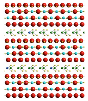
Scientists at The University of Manchester have ‘re-discovered’ a material, which could make the construction of 2D van der Waals heterostructures easier to build. Graphene was the world’s first two-dimensional material isolated in 2004 at The University of Manchester, it is 200 times stronger than steel, lightweight, flexible and more conductive than copper.
Since then a whole family of other 2D materials have been discovered and continues to grow. Using graphene and other 2D materials, scientists can layer these materials, similar to stacking bricks of Lego in a precisely chosen sequence known as van der Waals heterostructures to create high-performance structures tailored to a specific purpose.
One of the challenges when creating these heterostuctures is the painstaking stacking of the individual components on top of each other.
However, as reported in Nature Communications, a team supervised by Professor Robert Dryfe have discovered that franckeite (a mixed-metal sulphide mineral first discovered in 1893) naturally stacks into 2D sheets.
This results in van der Waals heterostructures, which can be exfoliated down to a single layer using simple scotch-tape mechanical exfoliation- the method used to isolate graphene. Importantly, this behaviour is likely to be common in a wider family of materials and could be exploited as an alternative to artificial stacking of two-dimensional materials.
Franckeite also opens us new possibilities for energy storage applications such as solar energy and supercapacitors due to its excellent electrical conductivity and remarkable electrochemical properties.
Research Associate Matěj Velický who led the experimental work said “We believe that this work will be followed by further studies of other natural van der Waals heterostructures and that the results will accelerate progress in the emerging “bottom-up” chemical synthesis of such complex structures”.
Prof Robert Dryfe said, “This work is a perfect demonstration of the continual surprises that are revealed through the study of 2D materials”.
Share on:


Suggested Items
Designer’s Notebook: What Designers Need to Know About Manufacturing, Part 2
04/24/2024 | Vern Solberg -- Column: Designer's NotebookThe printed circuit board (PCB) is the primary base element for providing the interconnect platform for mounting and electrically joining electronic components. When assessing PCB design complexity, first consider the component area and board area ratio. If the surface area for the component interface is restricted, it may justify adopting multilayer or multilayer sequential buildup (SBU) PCB fabrication to enable a more efficient sub-surface circuit interconnect.
Insulectro’s 'Storekeepers' Extend Their Welcome to Technology Village at IPC APEX EXPO
04/03/2024 | InsulectroInsulectro, the largest distributor of materials for use in the manufacture of PCBs and printed electronics, welcomes attendees to its TECHNOLOGY VILLAGE during this year’s IPC APEX EXPO at the Anaheim Convention Center, April 9-11, 2024.
ENNOVI Introduces a New Flexible Circuit Production Process for Low Voltage Connectivity in EV Battery Cell Contacting Systems
04/03/2024 | PRNewswireENNOVI, a mobility electrification solutions partner, introduces a more advanced and sustainable way of producing flexible circuits for low voltage signals in electric vehicle (EV) battery cell contacting systems.
Heavy Copper PCBs: Bridging the Gap Between Design and Fabrication, Part 1
04/01/2024 | Yash Sutariya, Saturn Electronics ServicesThey call me Sparky. This is due to my talent for getting shocked by a variety of voltages and because I cannot seem to keep my hands out of power control cabinets. While I do not have the time to throw the knife switch to the off position, that doesn’t stop me from sticking screwdrivers into the fuse boxes. In all honesty, I’m lucky to be alive. Fortunately, I also have a talent for building high-voltage heavy copper circuit boards. Since this is where I spend most of my time, I can guide you through some potential design for manufacturability (DFM) hazards you may encounter with heavy copper design.
Trouble in Your Tank: Supporting IC Substrates and Advanced Packaging, Part 5
03/19/2024 | Michael Carano -- Column: Trouble in Your TankDirect metallization systems based on conductive graphite or carbon dispersion are quickly gaining acceptance worldwide. Indeed, the environmental and productivity gains one can achieve with these processes are outstanding. In today’s highly competitive and litigious environment, direct metallization reduces costs associated with compliance, waste treatment, and legal issues related to chemical exposure. What makes these processes leaders in the direct metallization space?