


 It’s Only Common Sense: Nice Guys Really Can Finish First
 The Right Approach: I Hear the Train A Comin'
 Marcy's Musings: The Growing Industry
NASA and MIT Collaborate to Develop Space-Based Quantum-Dot Spectrometer
February 15, 2017 | NASAEstimated reading time: 3 minutes
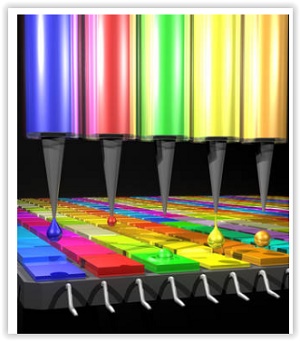
A NASA technologist has teamed with the inventor of a new nanotechnology that could transform the way space scientists build spectrometers, the all-important device used by virtually all scientific disciplines to measure the properties of light emanating from astronomical objects, including Earth itself.
Mahmooda Sultana, a research engineer at NASA’s Goddard Space Flight Center in Greenbelt, Maryland, now is collaborating with Moungi Bawendi, a chemistry professor at the Cambridge-based Massachusetts Institute of Technology, or MIT, to develop a prototype imaging spectrometer based on the emerging quantum-dot technology that Bawendi’s group pioneered.
NASA’s Center Innovation Fund, which supports potentially trailblazing, high-risk technologies, is funding the effort.
Introducing Quantum Dots
Quantum dots are a type of semiconductor nanocrystal discovered in the early 1980s. Invisible to the naked eye, the dots have proven in testing to absorb different wavelengths of light depending on their size, shape, and chemical composition. The technology is promising to applications that rely on the analysis of light, including smartphone cameras, medical devices, and environmental-testing equipment.
“This is as novel as it gets,” Sultana said, referring to the technology that she believes could miniaturize and potentially revolutionize space-based spectrometers, particularly those used on uninhabited aerial vehicles and small satellites. “It really could simplify instrument integration.”
Absorption spectrometers, as their name implies, measure the absorption of light as a function of frequency or wavelength due to its interaction with a sample, such as atmospheric gases.
After passing through or interacting with the sample, the light reaches the spectrometer. Traditional spectrometers use gratings, prisms, or interference filters to split the light into its component wavelengths, which their detector pixels then detect to produce spectra. The more intense the absorption in the spectra, the greater the presence of a specific chemical.
While space-based spectrometers are getting smaller due to miniaturization, they still are relatively large, Sultana said. “Higher-spectral resolution requires long optical paths for instruments that use gratings and prisms. This often results in large instruments. Whereas here, with quantum dots that act like filters that absorb different wavelengths depending on their size and shape, we can make an ultra-compact instrument. In other words, you could eliminate optical parts, like gratings, prisms, and interference filters.”
Just as important, the technology allows the instrument developer to generate nearly an unlimited number of different dots. As their size decreases, the wavelength of the light that the quantum dots will absorb decreases. “This makes it possible to produce a continuously tunable, yet distinct, set of absorptive filters where each pixel is made of a quantum dot of a specific size, shape, or composition. We would have precise control over what each dot absorbs. We could literally customize the instrument to observe many different bands with high-spectral resolution.”
Prototype Instrument Under Development
With her NASA technology-development support, Sultana is working to develop, qualify through thermal vacuum and vibration tests, and demonstrate a 20-by-20 quantum-dot array sensitive to visible wavelengths needed to image the sun and the aurora. However, the technology easily can be expanded to cover a broader range of wavelengths, from ultraviolet to mid-infrared, which may find many potential space applications in Earth science, heliophysics, and planetary science, she said.
Under the collaboration, Sultana is developing an instrument concept particularly for a CubeSat application and MIT doctoral student Jason Yoo is investigating techniques for synthesizing different precursor chemicals to create the dots and then printing them onto a suitable substrate. “Ultimately, we would want to print the dots directly onto the detector pixels,” she said.
“This is a very innovative technology,” Sultana added, conceding that it is very early in its development. “But we’re trying to raise its technology-readiness level very quickly. Several space-science opportunities that could benefit are in the pipeline.”
Share on:


Suggested Items
Warm Windows and Streamlined Skin Patches – IDTechEx Explores Flexible and Printed Electronics
04/26/2024 | IDTechExFlexible and printed electronics can be integrated into cars and homes to create modern aesthetics that are beneficial and easy to use. From luminous car controls to food labels that communicate the quality of food, the uses of this technology are endless and can upgrade many areas of everyday life.
iNEMI Packaging Tech Topic Series: Role of EDA in Advanced Semiconductor Packaging
04/26/2024 | iNEMIAdvanced semiconductor packaging with heterogenous integration has made on-package integration of multiple chips a crucial part of finding alternatives to transistor scaling. Historically, EDA tools for front-end and back-end design have evolved separately; however, design complexity and the increased number of die-to-die or die-to-substrate interconnections has led to the need for EDA tools that can support integration of overall design planning, implementation, and system analysis in a single cockpit.
Koh Young Showcases Award-winning Inspection Solutions at SMTconnect with SmartRep in Hall 4A.225
04/25/2024 | Koh Young TechnologyKoh Young Technology, the industry leader in True 3D measurement-based inspection solutions, will showcase an array of award-winning inspection and measurement solutions at SMTconnect alongside its sales partner, SmartRep, in booth 4A.225 at NürnbergMesse from June 11-13, 2023. The following offers a glimpse into what Koh Young will present at the tradeshow:
Real Time with… IPC APEX EXPO 2024: Plasmatreat: Innovative Surface Preparation Solutions
04/25/2024 | Real Time with...IPC APEX EXPOIn this interview, Editor Nolan Johnson speaks with Hardev Grewal, CEO and president of Plasmatreat, a developer of atmospheric plasma solutions. Plasmatreat uses clean compressed air and electricity to create plasma, offering environmentally friendly methods for surface preparation. Their technology measures plasma density for process optimization and can remove organic micro-contamination. Nolan and Hardev also discuss REDOX-Tool, a new technology for removing metal oxides.
Nanotechnology Market to Surpass $53.51 Billion by 2031
04/25/2024 | PRNewswireSkyQuest projects that the nanotechnology market will attain a value of USD 53.51 billion by 2031, with a CAGR of 36.4% over the forecast period (2024-2031).