


 It’s Only Common Sense: Nice Guys Really Can Finish First
 The Right Approach: I Hear the Train A Comin'
 Marcy's Musings: The Growing Industry
ULVAC Launches NA-1500 Dry Etching System for 600mm Advanced Packaging Substrate
March 21, 2017 | JCN NewswireEstimated reading time: 1 minute
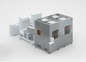
ULVAC, Inc. is pleased to introduce the NA-1500 dry etching system for 600mm advanced packaging substrates, providing for uniform Descum and Ti etching processes.
Higher data transfer speeds require high-density packaging technologies, while advanced mobile and wireless devices require thinner and higher-pin-count IC packages. Fan-Out Wafer Level Packaging (FO-WLP) is widespread, while Panel Level Packaging increases substrate size from 300mm to 600mm.
While there are many 200mm/300mm wafer dry etching systems in the market today, there was no dry etching system for 600mm substrate, providing for a uniform Descum process and Ti etching process. ULVAC developed the new system to address this need, and support mass-produced packaging processes.
The new NA-1500 dry etching system is made possible by enhancing our proven plasma source. Our plasma source enables fast, low-temperature etching in the resin layer, which had been previously impossible with existing CCP methods.
Our plasma source is also applicable to fluorine gases, so seed layer Ti etching, which requires a wet process, can proceed without side etching. SiO2 and SiN etching is available on the NA-1500 as well.
The NA-1500 dry etching system also provides stable transfer and processes without abnormal discharge, ensuringing warpage from the enlarged substrate is never an issue.
Applications:
1. Descum
2. Desmear
3. Surface treatment (Hydrophobicity <-> Hydrophilicity)
- Pretreatment for wet process such as plating, etc.
- Pretreatment for underfill
4. Resin material ashing
5. Seed layer Ti etching
6. SiO2/SiN etching
Our Future:
ULVAC has sold more than 200 dry etching systems since releasing our first 200mm wafer system 20 years ago. As electronic components become smaller and thinner, and higher-speed processing works on lower power in line with developments in IoT, manufacturing technologies for advanced packaging become more important. ULVAC supports this industry by providing systems that meet customer's future needs for flexible, invisible and wearable devices.
About ULVAC, Inc.
ULVAC, Inc., is a Japan-based vacuum equipment manufacturer. ULVAC was founded in 1952 and has contributed to development of industry and technology through comprehensive use of vacuum technology and its peripheral technology. We created "ULVAC SOLUTIONS" based on our one of a kind technologies built upon long years of research, development, and production technology innovations. We offer this solution composed of equipment, materials, analytic evaluation, vacuum components and other various services, for flat panel displays, solar cells, semiconductors, electronic components, and general industrial equipment.
Share on:


Suggested Items
Samsung Electronics Begins Industry’s First Mass Production of 9th-Gen V-NAND
04/29/2024 | Samsung ElectronicsSamsung Electronics, the world leader in advanced memory technology, today announced that it has begun mass production for its one-terabit (Tb) triple-level cell (TLC) 9th-generation vertical NAND (V-NAND), solidifying its leadership in the NAND flash market.
TSMC Celebrates 30th North America Technology Symposium
04/29/2024 | TSMCTSMC unveiled its newest semiconductor process, advanced packaging, and 3D IC technologies for powering the next generation of AI innovations with silicon leadership at the Company’s 2024 North America Technology Symposium.
QinetiQ Achieves UK’s First Jet-to-Jet Teaming Between Aircraft and Autonomous Drone
04/29/2024 | QinetiQQinetiQ has successfully trialled the UK’s first Crewed-Uncrewed-Teaming demonstration between a crewed aircraft and an autonomous jet drone.
Warm Windows and Streamlined Skin Patches – IDTechEx Explores Flexible and Printed Electronics
04/26/2024 | IDTechExFlexible and printed electronics can be integrated into cars and homes to create modern aesthetics that are beneficial and easy to use. From luminous car controls to food labels that communicate the quality of food, the uses of this technology are endless and can upgrade many areas of everyday life.
iNEMI Packaging Tech Topic Series: Role of EDA in Advanced Semiconductor Packaging
04/26/2024 | iNEMIAdvanced semiconductor packaging with heterogenous integration has made on-package integration of multiple chips a crucial part of finding alternatives to transistor scaling. Historically, EDA tools for front-end and back-end design have evolved separately; however, design complexity and the increased number of die-to-die or die-to-substrate interconnections has led to the need for EDA tools that can support integration of overall design planning, implementation, and system analysis in a single cockpit.