


 The Chemical Connection: Reducing Etch System Water Usage, Part 2
 It’s Only Common Sense: Nice Guys Really Can Finish First
 The Right Approach: I Hear the Train A Comin'
Researchers Make Major Breakthrough in Smart Printed Electronics
April 7, 2017 | AMBEREstimated reading time: 3 minutes
Researchers in AMBER, the Science Foundation Ireland-funded materials science research centre hosted in Trinity College Dublin, have fabricated printed transistors consisting entirely of 2-dimensional nanomaterials for the first time. These 2D materials combine exciting electronic properties with the potential for low-cost production. This breakthrough could unlock the potential for applications such as food packaging that displays a digital countdown to warn you of spoiling, wine labels that alert you when your white wine is at its optimum temperature, or even a window pane that shows the day’s forecast. The AMBER team’s findings have been published today in the leading journal Science*.
This discovery opens the path for industry, such as ICT and pharmaceutical, to cheaply print a host of electronic devices from solar cells to LEDs with applications from interactive smart food and drug labels to next-generation banknote security and e-passports.
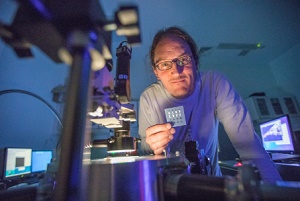
Prof Jonathan Coleman, who is an investigator in AMBER and Trinity’s School of Physics, said, “In the future, printed devices will be incorporated into even the most mundane objects such as labels, posters and packaging.
Printed electronic circuitry (constructed from the devices we have created) will allow consumer products to gather, process, display and transmit information: for example, milk cartons could send messages to your phone warning that the milk is about to go out-of-date.
We believe that 2D nanomaterials can compete with the materials currently used for printed electronics. Compared to other materials employed in this field, our 2D nanomaterials have the capability to yield more cost effective and higher performance printed devices. However, while the last decade has underlined the potential of 2D materials for a range of electronic applications, only the first steps have been taken to demonstrate their worth in printed electronics. This publication is important because it shows that conducting, semiconducting and insulating 2D nanomaterials can be combined together in complex devices. We felt that it was critically important to focus on printing transistors as they are the electric switches at the heart of modern computing. We believe this work opens the way to print a whole host of devices solely from 2D nanosheets.”
Led by Prof Coleman, in collaboration with the groups of Prof Georg Duesberg (AMBER) and Prof. Laurens Siebbeles (TU Delft,Netherlands), the team used standard printing techniques to combine graphene nanosheets as the electrodes with two other nanomaterials, tungsten diselenide and boron nitride as the channel and separator (two important parts of a transistor) to form an all-printed, all-nanosheet, working transistor.
Printable electronics have developed over the last thirty years based mainly on printable carbon-based molecules. While these molecules can easily be turned into printable inks, such materials are somewhat unstable and have well-known performance limitations. There have been many attempts to surpass these obstacles using alternative materials, such as carbon nanotubes or inorganic nanoparticles, but these materials have also shown limitations in either performance or in manufacturability. While the performance of printed 2D devices cannot yet compare with advanced transistors, the team believe there is a wide scope to improve performance beyond the current state-of-the-art for printed transistors.
The ability to print 2D nanomaterials is based on Prof. Coleman’s scalable method of producing 2D nanomaterials, including graphene, boron nitride, and tungsten diselenide nanosheets, in liquids, a method he has licensed to Samsung and Thomas Swan. These nanosheets are flat nanoparticles that are a few nanometres thick but hundreds of nanometres wide. Critically, nanosheets made from different materials have electronic properties that can be conducting, insulating or semiconducting and so include all the building blocks of electronics. Liquid processing is especially advantageous in that it yields large quantities of high quality 2D materials in a form that is easy to process into inks. Prof. Coleman’s publication provides the potential to print circuitry at extremely low cost which will facilitate a range of applications from animated posters to smart labels.
Prof Coleman is a partner in Graphene flagship, a €1 billion EU initiative to boost new technologies and innovation during the next 10 years.
Share on:


Suggested Items
LQDX Divests Aluminum Soldering Business - Mina™ - to Taiyo America Inc.
05/02/2024 | PRNewswireLQDX, formerly known as Averatek Corp., developer of high-performance materials for advanced semiconductor manufacturing, today announced that it has divested its aluminum soldering business – known as MinaTM – to Taiyo America Inc., a global market leader in advanced electronic materials.
Indium Corporation Expert to Present on Pb-Free Solder for Die-Attach in Discrete Power Applications
04/30/2024 | Indium CorporationIndium Corporation Product Manager – Semiconductor Dean Payne will present at the Advanced Packaging for Power Electronics conference, hosted by IMAPS, held May 8-9 in Woburn, Massachusetts, USA.
Real Time with... IPC APEX EXPO 2024: Adhesive Materials and Equipment Update with Dymax
05/01/2024 | Real Time with...IPC APEX EXPOVirginia Hogan, global business development manager at Dymax, discusses adhesive materials, dispensing and curing equipment, a new, high-reliability conformal coating, and various materials and dispensing methods.
Real Time with... IPC APEX EXPO 2024: Sustainability in the Industry
04/26/2024 | Real Time with...IPC APEX EXPOGuest Editor Henry Crandall and Chris Nash of Indium Corporation discuss the company's 90th anniversary and its focus on sustainability. They focus on the benefits of sustainable materials, their compatibility, and value propositions. The conversation also highlights how Durafuse LT technology's role in reducing reflow temperatures is leading to significant cost and energy savings. Nash also touches on downstream sustainability efforts such as using recycled materials for packaging.
SMC Korea 2024 to Highlight Semiconductor Materials Trends and Innovations on Industry’s Path to $1 Trillion
04/24/2024 | SEMIWith Korea a major consumer of semiconductor materials and advanced materials a key driver of innovation on the industry’s path to $1 trillion, industry leaders and experts will gather at SMC (Strategic Materials Conference) Korea 2024 on May 29 at the Suwon Convention Center in Gyeonggi-do, South Korea to provide insights into the latest materials developments and trends. Registration is open.