


 The Chemical Connection: Reducing Etch System Water Usage, Part 2
 It’s Only Common Sense: Nice Guys Really Can Finish First
 The Right Approach: I Hear the Train A Comin'
Better Living Through Pressure: Functional Nanomaterials Made Easy
April 20, 2017 | Sandia National LaboratoriesEstimated reading time: 3 minutes
Using pressure instead of chemicals, a Sandia National Laboratories team has fabricated nanoparticles into nanowire-array structures similar to those that underlie the surfaces of touch-screens for sensors, computers, phones and TVs. The pressure-based fabrication process takes nanoseconds. Chemistry-based industrial techniques take hours.
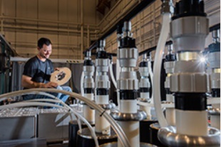
Sandia National Laboratories technologist Joshua Usher loads a target into the main power flow section of Veloce, a Sandia pulsed-power generator. The machine uses pressure rather than chemicals to form nanocomponents from nanoparticles. (Photo by Randy Montoya)
The process, called stress-induced fabrication, “is a new technology that mimics imprint processes already used by manufacturers,” said Sandia researcher Hongyou Fan, who led the effort. “Only instead of embossing credit cards, we’re using the same type of process to fabricate nanowires or other nano-sized components at ultrashort time scales.”
The method, for which three patents have been issued, is 9 million times faster than any known chemical method when performed on Sandia’s Veloce pulsed-power machine, which generates pressures on the order of 100,000 atmospheres, said Fan’s colleague, Jack Wise.
Less exotically, for manufacturing instead of research, embossing machines similar to those already commercially in use could serve. “It’s conceivable that few modifications would be needed to convert the machines from embossing to fabrication,” Fan said.
The Sandia process saves:
- time, because circuits can be fabricated in seconds instead of the hours required by chemical methods;
- the environment, because there’s no chemical waste to clean up;
- materials, because exactly the amount needed is placed on a substrate.
Also, defects common in industrial chemical fabrication of semiconductors are reduced in number by the pressure process, which acts to fill any vacancies occurring in the product’s atomic lattice.
“I have never seen or heard of this [process] in our extensive interaction with some of the leading material scientists in the world,” said Tom Brennan of Chicago-based Arch Venture Partners, speaking in a video about an earlier version of the process. “It allows us to think of completely new material solutions to problems industry is facing across the board.”
That earlier version of the pressure-based process worked by using a hand-tightened vise with diamond anvils, but that tool was not rapid or malleable enough for commercial production. Industrial embossing machines, on the other hand, produce sufficient pressure and are controllable.
“For a touch-screen, the pressure has to be worked out beforehand to stop the compression at just the right distance from the target: not too far, not too close, to produce the underlying nanowiring for a flat screen,” said Fan. “It’s a matter of programming the force applied to precisely determine how much to compress.”
That is, for flat screens, the nanowires need to be made flexible enough to contact an electrically charged layer of the device when pressed by a finger, yet far enough apart to remain separate when there’s no signal.
The technology, recently reported in Nature Communications, can fabricate a wide variety of nanoscale components including nanorods and nanosheets. The components can either be organized during their formation or dispersed in solvents for later assembly. The method could be used for chemical sensors, strain detectors and electrodes in solar cells.
Sandia researcher Hongyou Fan has been appointed a National Laboratory Professor at the University of New Mexico’s School of Engineering in its chemical and biological engineering department. The non-tenure-track appointment, which took effect March 1, automatically renews every three years and was made “in recognition of your significant achievements,” according to the university’s award notification. “I look forward to the opportunities for development of collaborative programs and student mentoring,” said Fan.
In addition to Fan and Wise, authors of the paper include Kaifu Bian, J. Matthew D. Lane, Gary S. Grest, Tommy Ao and Randy Hickman of Sandia; Zhongwu Wang from Cornell University; and former Sandia post-doctoral fellows Binsong Li and K. Michael Salerno.
The work was supported by the Department of Energy’s Office of Science. Part of the work was carried out at the Center for Integrated Nanotechnologies, a DOE Office of Science User Facility run by Sandia and Los Alamos national laboratories.
About Sandia National Laboratories
Sandia National Laboratories is a multimission laboratory operated by Sandia Corporation, a wholly owned subsidiary of Lockheed Martin Corp., for the U.S. Department of Energy’s National Nuclear Security Administration. With main facilities in Albuquerque, N.M., and Livermore, Calif., Sandia has major R&D responsibilities in national security, energy and environmental technologies and economic competitiveness.
Share on:


Suggested Items
Argonne, Toyota Collaborate on Cutting-Edge Battery Recycling Process
05/01/2024 | BUSINESS WIREThe U.S. Department of Energy’s (DOE) Argonne National Laboratory has recently launched a collaboration with Toyota Motor North America that could reduce the nation’s reliance on foreign sources of battery materials.
Real Time with… IPC APEX EXPO 2024: Outlining Rehm's Innovations and Global Presence
05/01/2024 | Real Time with...IPC APEX EXPOMichael Hanke, the chief sales officer for Rehm Thermal Systems, shares insights on the North American market, new machinery, and software development. He also discusses Rehm's turnkey solutions, process flexibility, global presence, and the dedicated team of 700 employees working on global solutions.
The Knowledge Base: A CM’s Perspective on Box Build Practices
04/30/2024 | Mike Konrad -- Column: The Knowledge BaseIn the ever-evolving landscape of electronics manufacturing, the box-build process stands out as a critical phase that bridges the gap between individual component manufacturing and the delivery of a fully functional electronic system. This intricate procedure, encompassing the assembly of everything from PCBs to wire harnesses and mechanical enclosures, demands a high level of precision, efficiency, and innovation. As the electronics assembly industry expands and diversifies, understanding the best practices within box-build assembly has become paramount for manufacturers aiming to stay ahead in a competitive market.
TSMC Certifies Ansys Multiphysics Platforms, Enabling Next-Gen AI and HPC Chips
04/30/2024 | PRNewswireAnsys announced the certification of its power integrity platforms for TSMC's N2 technology full production release. Both Ansys RedHawk-SC and Ansys Totem are certified for power integrity signoff on the N2 process, delivering significant speed and power advantages for high performance computing, mobile chips, and 3D-IC designs.
Koh Young Showcases Award-winning Inspection Solutions at SMTconnect with SmartRep in Hall 4A.225
04/25/2024 | Koh Young TechnologyKoh Young Technology, the industry leader in True 3D measurement-based inspection solutions, will showcase an array of award-winning inspection and measurement solutions at SMTconnect alongside its sales partner, SmartRep, in booth 4A.225 at NürnbergMesse from June 11-13, 2023. The following offers a glimpse into what Koh Young will present at the tradeshow: