


 The Chemical Connection: Reducing Etch System Water Usage, Part 2
 It’s Only Common Sense: Nice Guys Really Can Finish First
 The Right Approach: I Hear the Train A Comin'
Erasable Ink for 3D Printing
May 2, 2017 | KITEstimated reading time: 2 minutes
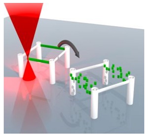
3D printing by direct laser writing produces micrometer-sized structures with precisely defined properties. Researchers of Karlsruhe Institute of Technology (KIT) have now developed a method to erase the ink used for 3D printing. In this way, the small structures of up to 100 nm in size can be erased and rewritten repeatedly. One nanometer corresponds to one millionth of a millimeter. This development opens up many new applications of 3D fabrication in biology or materials sciences, for instance.
Direct laser writing means that a computer-controlled, focused laser beam generates the structure in a photoresist similar to a pen. “Developing an ink that can be erased again was one of the big challenges in direct laser writing,” Professor Christopher Barner-Kowollik of KIT’s Institute for Chemical Technology and Polymer Chemistry says. The scientists have now met with success: They have developed an ink with reversible bonding, the building blocks of which can be separated from each other. The printed structure is simply erased by immersing it into a chemical solvent. At the point of erasure, a new structure can be written. In this way, the structure can be modified repeatedly.
The process was developed in close cooperation with the group of Professor Martin Wegener at the Institute of Applied Physics and the Institute of Nanotechnology of KIT. The physicists developed highly specialized 3D printers that produce scaffolds of up to 100 nm in size by direct laser writing.
“The ink with defined breaking points can be used for a variety of applications,” doctoral student and first author Markus Zieger says. Structures written with erasable ink can be integrated into structures made of non-erasable ink: Support constructions can be produced by 3D printing, which are similar to those used when building bridges and removed later on. It is also possible to further develop 3D designer petri dishes for use in biology. Recently, such structures were designed by KIT to grow cell cultures in three dimensions on the laboratory scale. “During cell growth, parts of the 3D microscaffold could be removed again to study how the cells react to the changed environment,” Martin Wegener explains. According to the scientists, it is also feasible to produce reversible wire bonds from erasable conducting structures in the future. A permanent ink can be mixed with a non-permanent ink to influence the properties of the printed material and make it more or less porous, for instance.
The new process is presented in the renowned journal Angewandte Chemie under the heading “Cleaving Direct Laser Written Microstructures on Demand.” The reviewers rated this publication a “very important paper.” 3D printing already is indispensable in many fabrication areas. Its importance is increasing. “According to estimations, some 10 percent of all goods will be produced by 3D printing in 2030,” Barner-Kowollik and Wegener say.
Markus M. Zieger, Patrick Mueller, Alexander S. Quick, Martin Wegener, Christopher Barner-Kowollik: Cleaving Direct Laser Written Microstructures on Demand. Angewandte Chemie 2017, 129, 1-6; DOI: 10.1002/anie.201701593
About Karlsruhe Institute of Technology (KIT)
Karlsruhe Institute of Technology (KIT) pools its three core tasks of research, higher education, and innovation in a mission. With about 9,300 employees and 25,000 students, KIT is one of the big institutions of research and higher education in natural sciences and engineering in Europe.
Share on:


Suggested Items
iNEMI Names Grace O'Malley CTO
05/02/2024 | iNEMIThe Board of Directors of the International Electronics Manufacturing Initiative (iNEMI) has named Grace O'Malley Chief Technical Officer (CTO).
Dubai Launches Global Blueprint for Artificial Intelligence
05/02/2024 | BUSINESS WIREDubai has launched a blueprint for Artificial Intelligence (AI), a yearly plan that will focus on harnessing the technology’s potential to improve quality of life around the world.
NextFlex Convenes the Hybrid Electronics Community at Binghamton University
05/01/2024 | NextFlexBinghamton University hosted the NextFlex hybrid electronics community on April 18 for a day of expert presentations, breakout sessions on technology and manufacturing topics, and networking.
IDTechEx Report on Quantum Technology: Nano-scale Physics for Massive Market Impact
04/30/2024 | PRNewswireThe quantum technology market leverages nano-scale physics to create revolutionary new devices for computing, sensing, and communications. Across the industry, quantum technology offers a paradigm shift in performance compared with incumbent solutions.
TSMC Certifies Ansys Multiphysics Platforms, Enabling Next-Gen AI and HPC Chips
04/30/2024 | PRNewswireAnsys announced the certification of its power integrity platforms for TSMC's N2 technology full production release. Both Ansys RedHawk-SC and Ansys Totem are certified for power integrity signoff on the N2 process, delivering significant speed and power advantages for high performance computing, mobile chips, and 3D-IC designs.