


 The Chemical Connection: Reducing Etch System Water Usage, Part 2
 It’s Only Common Sense: Nice Guys Really Can Finish First
 The Right Approach: I Hear the Train A Comin'
Stenciling with Atoms in Two-Dimensional Materials
May 2, 2017 | Penn State Materials Research InstituteEstimated reading time: 4 minutes
The possibilities for the new field of two-dimensional, one-atomic-layer-thick materials, including but not limited to graphene, appear almost limitless. In a new paper in the journal 2D Materials, Penn State researchers report two discoveries that will provide a simple and effective way to “stencil” high quality 2D materials in precise locations and overcome a barrier to their use in next-generation electronics.
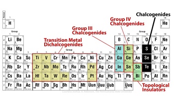
The discovery of a method to isolate a single atomic layer of carbon – graphene – in 2004 opened a new world of two-dimensional materials with properties not necessarily found in the familiar three-dimension world. Among these materials are a large group of elements that fall in the middle of the periodic table that are called transition metals. When atoms of certain transition metals, for instance molybdenum, are layered between two atomic layers of atoms from the chalcogenide elements, such as sulfur or selenium, the result is a three-layer sandwich called a transition metal dichalcogenide. TMDs have created tremendous interest among materials scientists because of their potential for new types of electronics, optoelectronics and computation.
“What we have focused on in this paper is the ability to make these materials over large areas of a substrate in precisely the places we want them,” says Joshua Robinson, associate professor of materials science and engineering. “These materials are of interest for a variety of next generation electronics, not necessarily to replace silicon, but to augment current technologies and ultimately to bring new chip functionality to silicon that we never had before.”
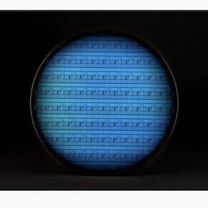
In order to integrate TMDs with silicon in transistors, chip companies will need to have a method to place the atoms precisely where they are needed. That method has not been available until now. In their 2D Materials paper, titled “Selective-area Growth and Controlled Substrate Coupling of Transition Metal Dichalcogenides,” Robinson and his group demonstrate for the first time a simple method of making precise patterns of two-dimensional materials using techniques familiar to any nanotechnology lab.
“It turns out the process is straight forward,” Robinson explains. “We spin photoresist on the sample in the cleanroom, as if we are going to start making a device. It can be any of a number of polymers that are used in nanofabrication. We then expose it to ultraviolet light in the desired areas, and we develop it like a photograph. Where the polymer was exposed to light, it washes away, and we then clean the surface further with standard plasma etching processes. The 2D materials will only grow in the areas that have been cleaned.”
A second simple discovery described in this work that could help advance the field of TMD research involves overcoming the strong effect a substrate has on the 2D materials grown on top of the substrate. In this case, molybdenum disulfide (MoS2), a highly studied semiconductor TMD, was grown on a sapphire substrate using typical powder-based deposition techniques. This resulted in the properties of the sapphire/MoS2 interface controlling the desired properties of the molybdenum disulfide, making it unsuitable for device fabrication.
“We needed to decouple the effects of the substrate on the 2D layer without transferring the layers off the sapphire,” says Robinson, “and so we simply tried dunking the as-grown material into liquid nitrogen and pulling it out into air to “crack” the interface. It turned out that was enough to separate the MoS2 from the sapphire and get closer to the intrinsic performance of the MoS2.”
The process is gentle enough to weaken the bonds connecting the 2D material to the substrate without completely setting it free. The exact mechanism for loosening the bonds is still under investigation, because of the complexity of this “simple process.” The two materials shrink at different rates, which could cause them to pop apart, but it could also be due to the bubbling of the liquid nitrogen as it turns into gas, or even contact with water vapor in the air that forms ice on the sample.
“We’re still working on understanding the exact mechanism, but we know that it works really well, at least with molybdenum disulfide,” Robinson says.
The three co-lead authors on the 2D Materials paper are Ph.D. students Brian Bersch and Yu-Chuan Lin, and research associate Sarah Eichfeld. Also contributing to this work are Robinson’s Ph.D. student Keohao Zhang and his former Ph.D. student, Ganesh Bhimanapati, now at Intel, undergraduate student Aleksander Piasecki, and Materials Research Institute staff scientist Michael Labella. Robinson is co-director of the Center for Atomically Thin Multifunctional Coatings (ATOMIC) and the Center for Two-Dimensional and Layered Materials (2DLM), and Director of User Programs for the Penn State 2D Crystal Consortium, all part of the Penn State Materials Research Institute.
The work was supported by the Center for Low Energy Systems Technology (LEAST), one of six Semiconductor Research STARnet centers, by the Defense Threat Reduction Agency and by the National Science Foundation.
Share on:


Suggested Items
Indium Corporation Expert to Present on Pb-Free Solder for Die-Attach in Discrete Power Applications
04/30/2024 | Indium CorporationIndium Corporation Product Manager – Semiconductor Dean Payne will present at the Advanced Packaging for Power Electronics conference, hosted by IMAPS, held May 8-9 in Woburn, Massachusetts, USA.
Real Time with... IPC APEX EXPO 2024: Adhesive Materials and Equipment Update with Dymax
05/01/2024 | Real Time with...IPC APEX EXPOVirginia Hogan, global business development manager at Dymax, discusses adhesive materials, dispensing and curing equipment, a new, high-reliability conformal coating, and various materials and dispensing methods.
Real Time with... IPC APEX EXPO 2024: Sustainability in the Industry
04/26/2024 | Real Time with...IPC APEX EXPOGuest Editor Henry Crandall and Chris Nash of Indium Corporation discuss the company's 90th anniversary and its focus on sustainability. They focus on the benefits of sustainable materials, their compatibility, and value propositions. The conversation also highlights how Durafuse LT technology's role in reducing reflow temperatures is leading to significant cost and energy savings. Nash also touches on downstream sustainability efforts such as using recycled materials for packaging.
SMC Korea 2024 to Highlight Semiconductor Materials Trends and Innovations on Industry’s Path to $1 Trillion
04/24/2024 | SEMIWith Korea a major consumer of semiconductor materials and advanced materials a key driver of innovation on the industry’s path to $1 trillion, industry leaders and experts will gather at SMC (Strategic Materials Conference) Korea 2024 on May 29 at the Suwon Convention Center in Gyeonggi-do, South Korea to provide insights into the latest materials developments and trends. Registration is open.
Groundbreaking Ceremony Marks the Beginning of a New Era for Newccess Industrial; The Construction of the MINGXIN Building
04/12/2024 | Newccess IndustrialOn a clear and sunny day in March, the groundbreaking ceremony for the MINGXIN Building took place in Shenzhen, China. This moment marked the official commencement of construction for a project that will reshape the semiconductor materials industry.