


 The Chemical Connection: Reducing Etch System Water Usage, Part 2
 It’s Only Common Sense: Nice Guys Really Can Finish First
 The Right Approach: I Hear the Train A Comin'
Holography With the Wi-Fi-Router
May 4, 2017 | Technical University of MunichEstimated reading time: 3 minutes
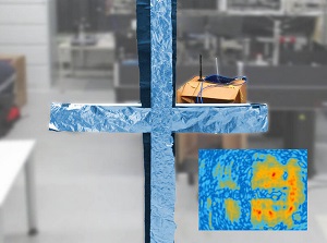
Scientists at the Technical University of Munich (TUM) have developed a holographic imaging process that depicts the radiation of a Wi-Fi transmitter to generate three-dimensional images of the surrounding environment. Industrial facility operators could use this to track objects as they move through the production hall.
Just like peering through a window, holograms project a seemingly three-dimensional image. While optical holograms require elaborate laser technology, generating holograms with the microwave radiation of a Wi-Fi transmitter requires merely one fixed and one movable antenna, as Dr. Friedenmann Reinhard and Philipp Holl report in the current issue of the renowned scientific journal Physical Review Letters.
“Using this technology, we can generate a three-dimensional image of the space around the Wi-Fi transmitter, as if our eyes could see microwave radiation,” says Friedemann Reinhard, director of the Emmy Noether Research Group for Quantum Sensors at the Walter Schottky Institute of the TU Munich. The researchers envision fields of deployment especially in the domain of industry 4.0 – automated industrial facilities, in which localizing parts and devices is often difficult.
Wi-Fi penetrates walls
Processes that allow the localization of microwave radiation, even through walls, or in which changes in a signal pattern signify the presence of a person already exist. The novelty is that an entire space can be imaged via holographic processing of Wi-Fi or cell phone signals.
“Of course, this raises privacy questions. After all, to a certain degree even encrypted signals transmit an image of their surroundings to the outside world,” says the project leader, Friedemann Reinhard. “However, it is rather unlikely that this process will be used for the view into foreign bedrooms in the near future. For that, you would need to go around the building with a large antenna, which would hardly go unnoticed. There are simpler ways available.”
Centimeter-scale precision
Hitherto, generating images from microwave radiation required special-purpose transmitters with large bandwidths. Using holographic data processing, the very small bandwidths of typical household Wi-Fi transmitters operating in the 2.4 and 5 gigahertz bands were sufficient for the researchers. Even Bluetooth and cell phone signals can be used. The wavelengths of these devices correspond to a spatial resolution of a few centimeters.
“Instead of a using a movable antenna, which measures the image point by point, one can use a larger number of antennas to obtain a video-like image frequency,” says Philipp Holl, who executed the experiments. “Future Wi-Fi frequencies, like the proposed 60 gigahertz IEEE 802.11 standard will allow resolutions down to the millimeter range.”
Looking to the future
Well-known optical methods for image processing can also be deployed in Wi-Fi holography: One example is the dark-field methodology used in microscopy, which improves the recognition of weakly diffracting structures. A further process is white-light holography in which the researchers use the remaining small bandwidth of the Wi-Fi transmitter to eliminated noise from scattered radiation.
The concept of treating microwave holograms like optical images allows the microwave image to be combined with camera images. The additional information extracted from the microwave images can be embedded into the camera image of a smart phone, for example to trace a radio tag attached to a lost item.
But the scientists are just at the beginning of the technological development. For example, research on the transparency of specific materials is lacking. This knowledge would facilitate the development of paint or wall paper translucent to microwaves for privacy protection, while transparent materials could be deployed in factory halls to allow parts to be tracked.
The researchers hope that further advancement of the technology may aid in the recovery of victims buried under an avalanche or a collapsed building. While conventional methods only allow point localization of victims, holographic signal processing could provide a spatial representation of destroyed structures, allowing first responders to navigate around heavy objects and use cavities in the rubble to systematically elucidate the easiest approach to quickly reach victims.
Share on:


Suggested Items
Merlin Flex invests in New Schmoll Direct Imaging System
04/30/2024 | Merlin Flex LtdMerlin Flex has fully installed and commissioned its 2nd Schmoll MDI Direct Imaging system. This new machine includes a twin bed, 4 head system which enhances Merlin Flex’s direct imaging capability for its 1.4M long flexible circuits.
Inkjet Solder Mask ‘Has Arrived’
04/10/2024 | Pete Starkey, I-Connect007I was delighted to be invited to attend an interactive webinar entitled “Solder Mask Coating Made Easy with Additive Manufacturing,” hosted by SUSS MicroTec Netherlands in Eindhoven. The webinar was introduced and moderated by André Bodegom, managing director at Adeon Technologies, and the speakers were Mariana Van Dam, senior product manager PCB imaging solutions at AGFA in Belgium; Ashley Steers, sales manager at Electra Polymers in the UK; and Dr. Luca Gautero, product manager at SUSS MicroTec Netherlands.
NetVia Group Acquires Direct Imaging from Mivatek
04/09/2024 | Miva TechnologiesMiva Technologies is pleased to announce NetVia Group, Irving, TX has acquired a new Miva 2400NG Dual Tray Direct Imaging System with 30-micron capabilities for inner, outer and soldermask imaging.
Teledyne to Acquire Adimec
02/13/2024 | TeledyneTeledyne Technologies Incorporated announced that it has entered into an agreement to acquire Adimec Holding B.V. and its subsidiaries.
Real Time with... productronica 2023: MivaTek Global Advances Technology With High-res Imaging System
12/08/2023 | Real Time with...productronicaMivaTek's Brendan Hogan talks about how the company employs Digitally Adaptive Rasterization Technology (DART) in their high-res imaging equipment. He also shares how the blurred line between semiconductors and microelectronics is driving broader application of the imaging process.