


 The Chemical Connection: Reducing Etch System Water Usage, Part 2
 It’s Only Common Sense: Nice Guys Really Can Finish First
 The Right Approach: I Hear the Train A Comin'
Laying the Foundations for Hybrid Silicon Lasers
June 16, 2017 | A*STAREstimated reading time: 2 minutes
Producing semiconductor lasers on a silicon wafer is a long-held goal for the electronics industry, but their fabrication has proved challenging. Now, researchers at A*STAR have developed an innovative way to manufacture them that is cheap, simple and scalable.
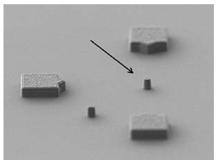
Oblique angle scanning electron microscopy image of a 500 nanometer diameter microdisk.
Hybrid silicon lasers combine the light-emitting properties of group III–V semiconductors, like gallium arsenide and indium phosphide, with the maturity of silicon manufacturing techniques. These lasers are attracting considerable attention as they promise inexpensive, mass-producible optical devices that can integrate with photonic and microelectronic elements on a single silicon chip. They have potential in a wide range of applications, from short-distance data communication to high-speed, long-distance optical transmission.
In the current production process, however, lasers are fabricated on separate III–V semiconductor wafers before being individually aligned to each silicon device — a time-consuming, costly process that limits the number of lasers that can be placed on a chip.
To overcome these limitations, Doris Keh-Ting Ng and her colleagues from the A*STAR Data Storage Institute have developed an innovative method for producing a hybrid III–V semiconductor and silicon-on-insulator (SOI) optical microcavity. This greatly reduces the complexity of the fabrication process and results in a more compact device.
“It’s very challenging to etch the entire cavity,” says Ng. “Currently, there is no single etch recipe and mask that allows the whole microcavity to be etched, and so we decided to develop a new approach.”
By first attaching a thin film of III–V semiconductor to a silicon oxide (SiO2) wafer using a SOI interlayer thermal bonding process, they produced a strong bond that also removes the need for strong oxidizing agents, such as Piranha solution or hydrofluoric acid.
And by using a dual hard-mask technique to etch the microcavity that confined etching to the intended layer, they eliminated the requirement to use multiple overlay lithography and etching cycles — a challenging procedure.
“Our approach cuts down the number of fabrication steps, reduces the use of hazardous chemicals, and requires only one lithography step to complete the process,” explains Ng.
The work presents, for the first time, a new heterocore configuration and integrated fabrication process that combines low-temperature SiO2 interlayer bonding with dual hard-mask, single lithography patterning.
“The process not only makes it possible to produce heterocore devices, it also greatly reduces the challenges of fabricating them, and could serve as an alternative hybrid microcavity for use by the research community,” says Ng.
Share on:


Suggested Items
Argonne, Toyota Collaborate on Cutting-Edge Battery Recycling Process
05/01/2024 | BUSINESS WIREThe U.S. Department of Energy’s (DOE) Argonne National Laboratory has recently launched a collaboration with Toyota Motor North America that could reduce the nation’s reliance on foreign sources of battery materials.
Real Time with… IPC APEX EXPO 2024: Outlining Rehm's Innovations and Global Presence
05/01/2024 | Real Time with...IPC APEX EXPOMichael Hanke, the chief sales officer for Rehm Thermal Systems, shares insights on the North American market, new machinery, and software development. He also discusses Rehm's turnkey solutions, process flexibility, global presence, and the dedicated team of 700 employees working on global solutions.
The Knowledge Base: A CM’s Perspective on Box Build Practices
04/30/2024 | Mike Konrad -- Column: The Knowledge BaseIn the ever-evolving landscape of electronics manufacturing, the box-build process stands out as a critical phase that bridges the gap between individual component manufacturing and the delivery of a fully functional electronic system. This intricate procedure, encompassing the assembly of everything from PCBs to wire harnesses and mechanical enclosures, demands a high level of precision, efficiency, and innovation. As the electronics assembly industry expands and diversifies, understanding the best practices within box-build assembly has become paramount for manufacturers aiming to stay ahead in a competitive market.
TSMC Certifies Ansys Multiphysics Platforms, Enabling Next-Gen AI and HPC Chips
04/30/2024 | PRNewswireAnsys announced the certification of its power integrity platforms for TSMC's N2 technology full production release. Both Ansys RedHawk-SC and Ansys Totem are certified for power integrity signoff on the N2 process, delivering significant speed and power advantages for high performance computing, mobile chips, and 3D-IC designs.
Koh Young Showcases Award-winning Inspection Solutions at SMTconnect with SmartRep in Hall 4A.225
04/25/2024 | Koh Young TechnologyKoh Young Technology, the industry leader in True 3D measurement-based inspection solutions, will showcase an array of award-winning inspection and measurement solutions at SMTconnect alongside its sales partner, SmartRep, in booth 4A.225 at NürnbergMesse from June 11-13, 2023. The following offers a glimpse into what Koh Young will present at the tradeshow: