


 The Chemical Connection: Reducing Etch System Water Usage, Part 2
 It’s Only Common Sense: Nice Guys Really Can Finish First
 The Right Approach: I Hear the Train A Comin'
Nickel for Thought: Compound Shows Potential for High-Temperature Superconductivity
June 26, 2017 | Argonne National LaboratoryEstimated reading time: 4 minutes
A team of researchers at the U.S. Department of Energy’s (DOE) Argonne National Laboratory has identified a nickel oxide compound as an unconventional but promising candidate material for high-temperature superconductivity.
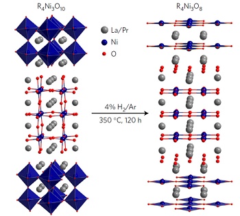
The team successfully synthesized single crystals of a metallic trilayer nickelate compound, a feat the researchers believe to be a first.
“It’s poised for superconductivity in a way not found in other nickel oxides. We’re very hopeful that all we have to do now is find the right electron concentration.”
This nickel oxide compound does not superconduct, said John Mitchell, an Argonne Distinguished Fellow and associate director of the laboratory’s Materials Science Division, who led the project, which combined crystal growth, X-ray spectroscopy, and computational theory. But, he added, “It’s poised for superconductivity in a way not found in other nickel oxides. We’re very hopeful that all we have to do now is find the right electron concentration.”
Superconducting materials are technologically important because electricity flows through them without resistance. High-temperature superconductors could lead to faster, more efficient electronic devices, grids that can transmit power without energy loss and ultra-fast levitating trains that ride frictionless magnets instead of rails.
Only low-temperature superconductivity seemed possible before 1986, but materials that superconduct at low temperatures are impractical because they must first be cooled to hundreds of degrees below zero. In 1986, however, discovery of high-temperature superconductivity in copper oxide compounds called cuprates engendered new technological potential for the phenomenon.
But after three decades of ensuing research, exactly how cuprate superconductivity works remains a defining problem in the field. One approach to solving this problem has been to study compounds that have similar crystal, magnetic and electronic structures to the cuprates.
Nickel-based oxides – nickelates – have long been considered as potential cuprate analogs because the element sits immediately adjacent to copper in the periodic table. Thus far, Mitchell noted, “That’s been an unsuccessful quest.” As he and his co-authors noted in their Nature Physics paper, “None of these analogs have been superconducting, and few are even metallic.”
The nickelate that the Argonne team has created is a quasi-two-dimensional trilayer compound, meaning that it consists of three layers of nickel oxide that are separated by spacer layers of praseodymium oxide.
“Thus it looks more two-dimensional than three-dimensional, structurally and electronically,” Mitchell said.
This nickelate and a compound containing lanthanum rather than praseodymium both share the quasi-two-dimensional trilayer structure. But the lanthanum analog is non-metallic and adopts a so-called “charge-stripe” phase, an electronic property that makes the material an insulator, the opposite of a superconductor.
“For some yet-unknown reason, the praseodymium system does not form these stripes,” Mitchell said. “It remains metallic and so is certainly the more likely candidate for superconductivity.”
Argonne is one of a few laboratories in the world where the compound could be created. The Materials Science Division’s high-pressure optical-image floating zone furnace has special capabilities. It can attain pressures of 150 atmospheres (equivalent to the crushing pressures found at oceanic depths of nearly 5,000 feet) and temperatures of approximately 2,000 degrees Celsius (more than 3,600 degrees Fahrenheit), conditions needed to grow the crystals.
“We didn’t know for sure we could make these materials,” said Argonne postdoctoral researcher Junjie Zhang, the first author on the study. But indeed, they managed to grow the crystals measuring a few millimeters in diameter (a small fraction of an inch).
The research team verified that the electronic structure of the nickelate resembles that of cuprate materials by taking X-ray absorption spectroscopy measurements at the Advanced Photon Source, a DOE Office of Science User Facility, and by performing density functional theory calculations. Materials scientists use density functional theory to investigate the electronic properties of condensed matter systems.
“I’ve spent my entire career not making high-temperature superconductors,” Mitchell joked. But that could change in the next phase of his team’s research: attempting to induce superconductivity in their nickelate material using a chemical process called electron doping, in which impurities are deliberately added to a material to influence its properties.
For the original study published in Nature Physics, see “Large orbital polarization in a metallic square-planar nickelate.” Other Argonne authors included Materials Science Division scientists Antia Botana, Daniel Phelan, Hong Zheng, Michael Norman, and John Freeland of the Advanced Photon Source; the other author was Victor Pardo of the University of Santiago de Compostela in Spain.
Funding was provided by the U.S. Department of Energy, Office of Science and the National Science Foundation.
Argonne National Laboratory seeks solutions to pressing national problems in science and technology. The nation's first national laboratory, Argonne conducts leading-edge basic and applied scientific research in virtually every scientific discipline. Argonne researchers work closely with researchers from hundreds of companies, universities, and federal, state and municipal agencies to help them solve their specific problems, advance America's scientific leadership and prepare the nation for a better future. With employees from more than 60 nations, Argonne is managed by UChicago Argonne, LLC for the U.S. Department of Energy's Office of Science.
The U.S. Department of Energy's Office of Science is the single largest supporter of basic research in the physical sciences in the United States and is working to address some of the most pressing challenges of our time.
Share on:


Suggested Items
The Chemical Connection: Reducing Etch System Water Usage, Part 2
05/02/2024 | Don Ball -- Column: The Chemical ConnectionIn my last column, I reviewed some relatively simple ways to reduce water usage in existing etch systems: cutting down cooling coil water flow, adding chillers to replace plant water for cooling, lowering flow rate nozzles for rinses, etc. This month, I’ll continue with more ways to control water usage in your etcher. Most of these are not easily retrofittable to existing equipment but should be given serious consideration when new equipment is contemplated. With the right combination of add-ons, it is possible to bring the amount of water used in an etch system to almost zero.
Designer’s Notebook: What Designers Need to Know About Manufacturing, Part 2
04/24/2024 | Vern Solberg -- Column: Designer's NotebookThe printed circuit board (PCB) is the primary base element for providing the interconnect platform for mounting and electrically joining electronic components. When assessing PCB design complexity, first consider the component area and board area ratio. If the surface area for the component interface is restricted, it may justify adopting multilayer or multilayer sequential buildup (SBU) PCB fabrication to enable a more efficient sub-surface circuit interconnect.
Insulectro’s 'Storekeepers' Extend Their Welcome to Technology Village at IPC APEX EXPO
04/03/2024 | InsulectroInsulectro, the largest distributor of materials for use in the manufacture of PCBs and printed electronics, welcomes attendees to its TECHNOLOGY VILLAGE during this year’s IPC APEX EXPO at the Anaheim Convention Center, April 9-11, 2024.
ENNOVI Introduces a New Flexible Circuit Production Process for Low Voltage Connectivity in EV Battery Cell Contacting Systems
04/03/2024 | PRNewswireENNOVI, a mobility electrification solutions partner, introduces a more advanced and sustainable way of producing flexible circuits for low voltage signals in electric vehicle (EV) battery cell contacting systems.
Heavy Copper PCBs: Bridging the Gap Between Design and Fabrication, Part 1
04/01/2024 | Yash Sutariya, Saturn Electronics ServicesThey call me Sparky. This is due to my talent for getting shocked by a variety of voltages and because I cannot seem to keep my hands out of power control cabinets. While I do not have the time to throw the knife switch to the off position, that doesn’t stop me from sticking screwdrivers into the fuse boxes. In all honesty, I’m lucky to be alive. Fortunately, I also have a talent for building high-voltage heavy copper circuit boards. Since this is where I spend most of my time, I can guide you through some potential design for manufacturability (DFM) hazards you may encounter with heavy copper design.