


 The Chemical Connection: Reducing Etch System Water Usage, Part 2
 It’s Only Common Sense: Nice Guys Really Can Finish First
 The Right Approach: I Hear the Train A Comin'
New Class of ‘Soft’ Semiconductors Could Transform HD Displays
June 27, 2017 | Berkeley LabEstimated reading time: 4 minutes
A new type of semiconductor may be coming to a high-definition display near you. Scientists at the Department of Energy’s Lawrence Berkeley National Laboratory (Berkeley Lab) have shown that a class of semiconductor called halide perovskites is capable of emitting multiple, bright colors from a single nanowire at resolutions as small as 500 nanometers.
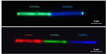
Single nanowires shown emitting different colors. The top panel shows a cesium lead bromide (CsPbBr3)-cesium lead chloride (CsPbCl3) heterojunction simultaneously emitting green and blue lights, respectively, under UV excitation. The bottom panel shows a cesium lead iodide (CsPbI3)-cesium lead bromide-cesium lead chloride configuration emitting red, green, and blue lights, respectively. (Credit: Letian Dou/Berkeley Lab and Connor G. Bischak/UC Berkeley)
The findings, published online this week in the early edition of the Proceedings of the National Academy of Sciences, represent a clear challenge to quantum dot displays that rely upon traditional semiconductor nanocrystals to emit light. It could also influence the development of new applications in optoelectronics, photovoltaics, nanoscopic lasers, and ultrasensitive photodetectors, among others.
The researchers used electron beam lithography to fabricate halide perovskite nanowire heterojunctions, the junction of two different semiconductors. In device applications, heterojunctions determine energy level and bandgap characteristics, and are therefore considered a key building block of modern electronics and photovoltaics.
The researchers pointed out that the lattice in halide perovskites is held together by ionic instead of covalent bonds. In ionic bonds, atoms of opposite charges are attracted and transfer electrons to each other. Covalent bonds, in contrast, occur when atoms share their electrons with each other.
“With inorganic halide perovskites, we can easily swap the anions in the ionic bonds while maintaining the single crystalline nature of the materials,” said study principal investigator Peidong Yang, senior faculty scientist at Berkeley Lab’s Materials Sciences Division. “This allows us to easily reconfigure the structure and composition of the material. That’s why halide perovskites are considered soft lattice semiconductors. Covalent bonds, in contrast, are relatively robust and require more energy to change. Our study basically showed that we can pretty much change the composition of any segment of this soft semiconductor.”
A 2-D plate showing alternating cesium lead chloride (blue) and cesium lead bromide (green) segments. (Credit: Letian Dou/Berkeley Lab and Connor G. Bischak/UC Berkeley)
In this case, the researchers tested cesium lead halide perovskite, and then they used a common nanofabrication technique combined with anion exchange chemistry to swap out the halide ions to create cesium lead iodide, cesium lead bromide, and cesium lead chloride perovskites.
Each variation resulted in a different color emitted. Moreover, the researchers showed that multiple heterojunctions could be engineered on a single nanowire. They were able to achieve a pixel size down to 500 nanometers, and they determined that the color of the material was tunable throughout the entire range of visible light.
The researchers said that the chemical solution-processing technique used to treat this class of soft, ionic-bonded semiconductors is far simpler than methods used to manufacture traditional colloidal semiconductors.
“For conventional semiconductors, fabricating the junction is quite complicated and expensive,” said study co-lead author Letian Dou, who conducted the work as a postdoctoral fellow in Yang’s lab. “High temperatures and vacuum conditions are usually involved to control the materials’ growth and doping. Precisely controlling the materials composition and property is also challenging because conventional semiconductors are ‘hard’ due to strong covalent bonding.”
To swap the anions in a soft semiconductor, the material is soaked in a special chemical solution at room temperature.
“It’s a simple process, and it is very easy to scale up,” said Yang, who is also a professor of chemistry at UC Berkeley. “You don’t need to spend long hours in a clean room, and you don’t need high temperatures.”
The researchers are continuing to improve the resolution of these soft semiconductors, and are working to integrate them into an electric circuit.
Other co-lead authors on this paper are Christopher Kley, UC Berkeley postdoctoral fellow, and Minliang Lai, UC Berkeley graduate student. Dou is now an assistant professor of chemical engineering at Purdue University.
The DOE Office of Science supported this work.
About Lawrence Berkeley National Laboratory
Lawrence Berkeley National Laboratory addresses the world’s most urgent scientific challenges by advancing sustainable energy, protecting human health, creating new materials, and revealing the origin and fate of the universe. Founded in 1931, Berkeley Lab’s scientific expertise has been recognized with 13 Nobel Prizes. The University of California manages Berkeley Lab for the U.S. Department of Energy’s Office of Science. For more, visit www.lbl.gov.
About DOE’s Office of Science
DOE’s Office of Science is the single largest supporter of basic research in the physical sciences in the United States, and is working to address some of the most pressing challenges of our time. For more information, please visit science.energy.gov.
Share on:


Suggested Items
Seeking Employment: Palash Pranav Vyas
05/03/2024 | Barry Matties, I-Connect007Despite skilled worker shortages across the industry, there are many educated and qualified individuals ready to contribute to electronics manufacturing. Here we profile Palash Pranav Vyas, a Ph.D. candidate at Auburn University whose work in drop shock reliability won him Best Student Poster at IPC APEX EXPO 2024.
Koh Young Extends Invitation to the 2024 IEEE Electronic Components and Technology Conference
04/30/2024 | Koh YoungKoh Young, the industry leader in True3D measurement-based inspection solutions, invites you to join us at the at the 2024 IEEE Electronic Components and Technology Conference from May 28-31, 2024, in Denver, Colorado at the Gaylord Rockies Resort & Convention Center.
Real Time with... IPC APEX EXPO 2024: Sustainability in the Industry
04/26/2024 | Real Time with...IPC APEX EXPOGuest Editor Henry Crandall and Chris Nash of Indium Corporation discuss the company's 90th anniversary and its focus on sustainability. They focus on the benefits of sustainable materials, their compatibility, and value propositions. The conversation also highlights how Durafuse LT technology's role in reducing reflow temperatures is leading to significant cost and energy savings. Nash also touches on downstream sustainability efforts such as using recycled materials for packaging.
I-Connect007 Editor’s Choice: Five Must-Reads for the Week
04/26/2024 | Andy Shaughnessy, Design007 MagazineIn this week’s roundup, we have a variety of articles covering everything from design through assembly, and even box build. I’ve always wondered whether box build was all it was cracked up to be. Do customers really pick one EMS provider over another because one company offers box build? And if you’ve ever wanted to volunteer, IPC’s Thought Leaders Program is looking for a few good technologists to help them on their mission. Check out Stanton Rak’s article, which was published in the spring issue of IPC Community.
Taiyo Circuit Automation Installs New DP3500 into Fuba Printed Circuits, Tunisia
04/25/2024 | Taiyo Circuit AutomationTaiyo Circuit Automation is proud to be partnered with Fuba Printed Circuits, Tunisia part of the OneTech Group of companies, a leading printed circuit board manufacturer based out of Bizerte, Tunisia, on their first installation of Taiyo Circuit Automation DP3500 coater.