


 The Government Circuit: Driving Resiliency and Economic Security on Both Sides of the Atlantic
 American Made Advocacy: Taking the Fight to Capitol Hill
 Defense Speak Interpreted: SWaPing Nanosatellites for Defense Systems
Evaluation of Stencil Technology for Miniaturization
December 22, 2017 | Neeta Agarwal, et al.*Estimated reading time: 4 minutes
SMT stencil printing technology continually evolves to keep pace with device miniaturization technologies. Printed circuit board assemblers have numerous new technology options to choose from, and need to determine the most effective ones to produce the highest quality and most reliable solder interconnections.
The objective of these tests was to identify the best stencil technology for high-volume production of miniaturized SMT components. The solder paste used for this assessment was SAC305 Pb-free no-clean, Type 4 mesh. The specified stencil thickness for all stencils was 4 mils (100μm).
EXPERIMENTAL SETUP
Test Vehicle
The test vehicle shown in Figure 1 was designed in-house for a multitude of PCB assembly tests, including new packages, pad designs, solder paste print performance and process evaluation tests. The devices selected for analysis in these tests included 0.3- and 0.4 mm-pitch BGAs and 0201s. Their area ratios ranged from 0.46 to 0.70. Locations and names of the specific devices used in the stencil analysis are shown in Figure 1.
Figure 1: Test vehicle and features used in stencil analysis.
The recommended stencil thickness for the 0.3mm microBGA location is 3 mils (75 μm) versus the 4 mil (100 μm) thickness selected for this study. Consistent release for these apertures was not anticipated but relative comparisons of release would provide an indication of stencil performance.
Test Design
The stencil analysis included:
- 6 different stencil suppliers
- 9 different foil materials
- 5 different manufacturing processes
- 7 different nanocoatings
The experimental design was not a full factorial. Each supplier provided stencils using technologies that were either their top performers (high end), developmental technologies that they wanted to learn more about (supplier choices #1 and #2), or lower cost stencils commonly ordered (AR>0.70). One to four stencils were submitted by each supplier. A total of 18 stencils were print tested. All were created using the same Gerber file, and all were specified at 0.0040” thick with identical apertures depending on the feature.
The Benchmark test vehicles were printed at the Benchmark Electronic Inc., Nashua, New Hampshire facility on a DEK 265 screen printer utilizing 18 stencils over a duration of three days. The solder paste was Pb-free, SAC305 no clean, Type 4 mesh. For each stencil, a total of six boards with a 10-minute delay between prints were printed by the same operator, using identical and common machine print parameters. The cards were printed in the same order and the underside of stencil was dry wiped after each print. All boards were measured with a Koh Young solder paste inspection (SPI) platform. The 1st and 6th boards were photographed to provide a visual assessment of print repeatability; these images appear in Appendix I. Each stencil was photographed after completion of the dry wipe following the 6th print. These images also appear in Appendix I and provide a relative comparison of paste release. Specifically, stencil apertures with the less amounts of paste indicate better release.
Stencil Assessment Criteria
This study incorporated multiple parameters to assess stencil performance:
- Dimensional accuracy of the aperture opening or size accuracy
- Visual assessment of the print and stencil after the final print to determine the amount of paste remaining in the apertures
- Topography of the aperture walls
- Analysis of SPI data for transfer efficiency and repeatability
Size Accuracy of the Apertures
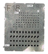
Miniature components require apertures that are within specification. Apertures that are too small increase the risk of insufficient solder defects due to poor paste release and apertures that are too large increase the risk of bridging and solder balls. Inconsistent apertures on 01005 or 0201 components increase the risk of tombstoning. The stencil providers were asked to include four small coupons outside the print area that could be removed and measured for accuracy and topography assessment. The latter is a destructive test. A stencil coupon is shown in Figure 2.
Figure 2: Stencil coupon for F18.
The coupon has 11 rows with various aperture openings in terms of size and shape, representing various components. Each row has 10 identical apertures to provide an indication of repeatability. The first row is a circular aperture with a specified diameter of 7.3 mils and the 2nd row is a square aperture with a specified length and width of 7.3 mils. These two rows are nearest the typical aperture for a 01005 component. The top side and bottom sides of the coupon were measured at Vicor using a Keyence digital microscope. The location of the aperture relative to the fiducial, or location accuracy, was not measured in this study. Each measurement was ranked as target condition (green), acceptable (yellow), or unacceptable (red). A green aperture measured within ±.3 mils to the specification, a yellow was within ±.3 to .5 mils, and red was outside of ±.5 mils. The number of green, yellow and red ratings for each stencil was tabulated and the stencils ranked based on this criteria. The most accurate stencils did not have red ratings, and were ranked based on the highest number of green and fewest number of yellow ratings. The stencils with red ratings were ranked in descending order based on the number of red ratings.
If two stencils had the same amount of red ratings, the number of green and yellow ratings was used to delineate the ranking.
Visual Assessment of Print and Stencil
The visual assessments of paste deposits after the first and sixth print were performed at two selected fine pitch component pads 0.3 mm microBGA and 0.4 mm microBGA locations. Each stencil was also inspected after the final (sixth) print to have perspective on the amount of paste remaining in the apertures. The photos of uncleaned stencil apertures/windows at the same two component locations were also recorded after last or 6th print.
To read the full version of this article, which appeared in the December 2017 issue of SMT Magazine, click here.
Share on:


Suggested Items
Indium Experts to Present on High-Temperature, Lead-Free Solder Paste and High Reliability Liquid Metal Alloys Poster at ECTC
05/16/2024 | Indium CorporationIndium Corporation Research Associate Kyle Aserian will deliver a presentation at the 74th Electronic Components and Technology Conference (ECTC) on May 31, in Denver, Colorado.
Indium Experts to Present at Electronics in Harsh Environments SMTA Conference
05/13/2024 | Indium Corporationndium Corporation Technical Manager for Europe, Africa, and the Middle East, Karthik Vijay, will deliver a technical presentation and Indium Corporation Senior Technologist, Dr. Ronald Lasky, will deliver both a workshop and technical presentation at the Electronics in Harsh Environments SMTA Conference on May 14-16 in Copenhagen, Denmark.
Connect the Dots: Designing for Reality—The Pre-Manufacturing Process
05/08/2024 | Matt Stevenson -- Column: Connect the DotsI have been working with Nolan Johnson on a podcast series about designing PCBs for the reality of manufacturing. By sharing lessons learned over a long career in the PCB industry, we hope to shorten learning curves and help designers produce better boards with less hassle and rework. Episode 2 deals with the electronic pre-manufacturing process. Moving from CAD (computer-aided design) to CAM (computer-aided manufacturing) is a key step in PCB manufacturing. CAM turns digital designs into instructions that machines can use to actually build the PCB.
AIM Solder Signs Shinil Fl Ltd. as New Distributor for Korea
05/08/2024 | AIM SolderAIM Solder, a leading global manufacturer of solder assembly materials for the electronics industry, is pleased to announce a new distribution partnership with Shinil Fl Ltd., a prominent supplier of technological solutions in the SMT and semiconductor sectors.
Indium Corporation to Showcase HIA Materials at ECTC
05/07/2024 | Indium CorporationAs an industry leader in innovative materials solutions for semiconductor packaging and assembly, Indium Corporation® will feature its advanced products designed to meet the evolving challenges of heterogeneous integration and assembly (HIA) and fine-pitch system-in-package (SiP) applications at the 74th Electronic Components and Technology Conference (ECTC), May 28‒31, in Denver, Colorado.