


 American Made Advocacy: What About the Rest of the Technology Stack?
 It’s Only Common Sense: Great Ideas From John Mitchell’s Book on Hiring Habits
 Punching Out: Breaking Out of the Valuation Box
Study Reveals New Insights into How Hybrid Perovskite Solar Cells Work
March 21, 2018 | SLAC National Accelerator LaboratoryEstimated reading time: 6 minutes
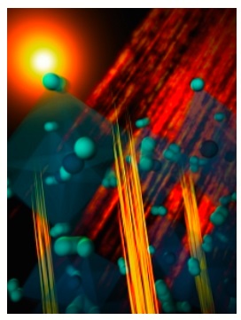
Scientists have gained new insights into a fundamental mystery about hybrid perovskites, low-cost materials that could enhance or even replace conventional solar cells made of silicon.
Under a microscope, a slice of perovskite looks like an abstract mosaic of random grains of crystal. The mystery is how this patchwork of tiny, imperfect grains can transform sunlight into electricity as efficiently as a single crystal of pure silicon.
A recent study by scientists at Stanford University and the Department of Energy’s SLAC National Accelerator Laboratory offers new clues. Writing in the March 15th issue of Advanced Materials, the scientists provide a new understanding of how electric charges separate in perovskites a few billionths of a second following the absorption of light, the crucial first step in generating an electric current.
The study is the first to probe the inner workings of hybrid perovskites at the atomic scale using laser pulses that match the intensity of solar radiation, and thus mimic natural sunlight. The authors say their discovery could lead to improvements in the performance of perovskite solar cells and a new way to probe their functionality.
Perovskites and Silicon
Most solar cells today are made of purified silicon manufactured at temperatures above 3,000 degrees Fahrenheit (1,600 degrees Celsius). These rigid silicon panels can last for decades in all kinds of weather conditions.
Perovskite solar cells, although far less durable, are thinner and more flexible than silicon cells and can be produced near room temperature from a hybrid mixture of cheap organic and inorganic materials, like iodine, lead and methylammonium.
Researchers, including Stanford co-author Michael McGehee, have shown that perovskite solar cells are as efficient at converting light to electricity as commercially available silicon cells and can even outperform them. This combination of efficiency, flexibility and easy synthesis has fueled a worldwide race to develop commercial-grade perovskites that can withstand long-term exposure to heat and precipitation.
“Perovskites are very promising materials for photovoltaics,” said lead author Burak Guzelturk, a postdoctoral scholar at Stanford and SLAC. “But people wonder how they can achieve such high efficiencies.”
Electrons and Holes
All solar cells operate on the same principle. Photons of sunlight absorbed by the crystalline material kick negatively charged electrons into an excited state. The freed electrons leave behind positively charged spaces or “holes” that separate from one another. This separation gives rise to an electric current.
Pure silicon, with its highly ordered atomic structure, provides a direct path for electrons and holes to travel through the solar cell. But with perovskites, the road is far from smooth.
“Perovskites are typically filled with defects,” said co-author Aaron Lindenberg, an associate professor at SLAC and Stanford and investigator with the Stanford Institute of Materials and Energy Sciences (SIMES). “They’re not even close to being perfect crystals, yet somehow the electric currents don’t see the defects.”
Terahertz Emission
For the study, the research team used laser pulses to simulate waves of sunlight from both ends of the visible light spectrum – high-energy violet light and low-energy infrared light. The results were measured at the picosecond timescale. One picosecond is one trillionth of a second.
“In the first picoseconds after sunlight hits the perovskite, the electrons and holes in the crystalline lattice start to split,” Lindenberg explained. “The separation was uncovered by measuring the emission of high-frequency terahertz light pulses oscillating a trillion times per second from the perovskite thin film. This is the first time anyone has observed terahertz emission from hybrid perovskites.”
The terahertz emission also revealed that electrons and holes closely interact with lattice vibrations in the crystalline material. This interaction, which occurs on a femtosecond timescale, could help explain how electric currents navigate through the patchwork of crystal grains in hybrid perovskites.
"As the electric charges separate, we observe a sharp spike in the terahertz emission, matching a vibrational mode of the material,” Guzelturk said. “That gives us clear evidence that the electrons and holes are strongly coupling with the atomic vibrations in the material.”
This finding raises the possibility that coupling to the lattice vibration could protect the electrons and holes from charged defects in the perovskite, shielding the electric current as it travels through the solar cell. Similar scenarios have been proposed by other research teams.
“This is one of the first observations of how the local atomic structure of a hybrid perovskite material responds in the first trillionths of a second after absorbing sunlight,” Lindenberg said. “Our technique could open up a new way of probing a solar cell right when the photon is absorbed, which is really important if you want to understand and build better materials. The conventional way is to put electrodes on the device and measure the current, but that essentially blurs out all of the microscopic processes that are key. Our all-optical, electrode-less approach with femtosecond time resolution avoids that problem.”
Page 1 of 2
Share on:


Suggested Items
IPC APEX EXPO: Some Thoughts About Growth
05/16/2024 | Dan Feinberg, I-Connect007After two and a half days of wandering the aisles at IPC APEX EXPO 2024, for the first time, I almost felt like I was exploring CES. There were so many booths and exhibits that I could describe, but I’d like to focus on the growth and huge value of this event, which has expanded well beyond just the growing and impressive exhibit show floor.
The Shaughnessy Report: Unlock Your High-speed Material Constraints
05/15/2024 | Andy Shaughnessy -- Column: The Shaughnessy ReportThe world of PCB materials used to be a fairly simple one. It was divided into two groups: the “traditional” laminates, often called FR-4, and the high-speed laminates developed especially for high-speed PCBs. These were two worlds that usually didn’t collide. But then traditional laminates started getting better, and high-speed designers and design engineers took notice and started to reconsider what FR-4 could be used for.
Breaking High-speed Material Constraints: Design007 Magazine — May 2024
05/14/2024 | I-Connect007 Editorial TeamDo you need specialty materials for your high-speed designs? Maybe not. Improvements in resins mean designers of high-speed boards can sometimes use traditional laminate systems instead of high-speed materials, saving time and money while streamlining the fab process. In the May 2024 issue of Design007 Magazine, our contributors explain how to avoid overconstraining your materials when working with high-speed boards.
Indium Experts to Present at Electronics in Harsh Environments SMTA Conference
05/13/2024 | Indium Corporationndium Corporation Technical Manager for Europe, Africa, and the Middle East, Karthik Vijay, will deliver a technical presentation and Indium Corporation Senior Technologist, Dr. Ronald Lasky, will deliver both a workshop and technical presentation at the Electronics in Harsh Environments SMTA Conference on May 14-16 in Copenhagen, Denmark.
Ansys’ Collaboration with Schrödinger will Accelerate Materials Development with Unprecedented Multiscale Simulation
05/09/2024 | ANSYSAnsys and Schrödinger are collaborating to deliver an ICME approach that bridges the gap between materials discovery and product development.