


 Material Insight: The Dielectric Constant of PCB Materials
 American Made Advocacy: What About the Rest of the Technology Stack?
 It’s Only Common Sense: Great Ideas From John Mitchell’s Book on Hiring Habits
New Quantum Materials Could Take Computers Beyond the Semiconductor Era
December 4, 2018 | UC BerkeleyEstimated reading time: 5 minutes
Researchers from Intel Corp. and UC Berkeley are looking beyond current transistor technology and preparing the way for a new type of memory and logic circuit that could someday be in every computer on the planet.
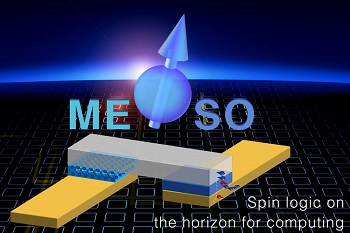
Image Caption: MESO devices, based on magnetoelectric and spin-orbit materials, could someday replace the ubiquitous semiconductor transistor, today represented by CMOS. MESO uses up-and-down magnetic spins in a multiferroic material to store binary information and conduct logic operations. (Intel graphic)
In a paper appearing online Dec. 3 in advance of publication in the journal Nature, the researchers propose a way to turn relatively new types of materials, multiferroics and topological materials, into logic and memory devices that will be 10 to 100 times more energy-efficient than foreseeable improvements to current microprocessors, which are based on CMOS (complementary metal–oxide–semiconductor).
The magneto-electric spin-orbit or MESO devices will also pack five times more logic operations into the same space than CMOS, continuing the trend toward more computations per unit area, a central tenet of Moore’s Law.
The new devices will boost technologies that require intense computing power with low energy use, specifically highly automated, self-driving cars and drones, both of which require ever increasing numbers of computer operations per second.
“As CMOS develops into its maturity, we will basically have very powerful technology options that see us through. In some ways, this could continue computing improvements for another whole generation of people,” said lead author Sasikanth Manipatruni, who leads hardware development for the MESO project at Intel’s Components Research group in Hillsboro, Oregon. MESO was invented by Intel scientists, and Manipatruni designed the first MESO device.
Transistor technology, invented 70 years ago, is used today in everything from cellphones and appliances to cars and supercomputers. Transistors shuffle electrons around inside a semiconductor and store them as binary bits 0 and 1.
Single crystals of the multiferroic material bismuth-iron-oxide. The bismuth atoms (blue) form a cubic lattice with oxygen atoms (yellow) at each face of the cube and an iron atom (gray) near the center. The somewhat off-center iron interacts with the oxygen to form an electric dipole (P), which is coupled to the magnetic spins of the atoms (M) so that flipping the dipole with an electric field (E) also flips the magnetic moment. The collective magnetic spins of the atoms in the material encode the binary bits 0 and 1, and allow for information storage and logic operations.
In the new MESO devices, the binary bits are the up-and-down magnetic spin states in a multiferroic, a material first created in 2001 by Ramamoorthy Ramesh, a UC Berkeley professor of materials science and engineering and of physics and a senior author of the paper.
“The discovery was that there are materials where you can apply a voltage and change the magnetic order of the multiferroic,” said Ramesh, who is also a faculty scientist at Lawrence Berkeley National Laboratory. “But to me, ‘What would we do with these multiferroics?’ was always a big question. MESO bridges that gap and provides one pathway for computing to evolve”.
In the Nature paper, the researchers report that they have reduced the voltage needed for multiferroic magneto-electric switching from 3 volts to 500 millivolts, and predict that it should be possible to reduce this to 100 millivolts: one-fifth to one-tenth that required by CMOS transistors in use today. Lower voltage means lower energy use: the total energy to switch a bit from 1 to 0 would be one-tenth to one-thirtieth of the energy required by CMOS.
“A number of critical techniques need to be developed to allow these new types of computing devices and architectures,” said Manipatruni, who combined the functions of magneto-electrics and spin-orbit materials to propose MESO. “We are trying to trigger a wave of innovation in industry and academia on what the next transistor-like option should look like.”
Page 1 of 2
Share on:


Suggested Items
Material Insight: The Dielectric Constant of PCB Materials
05/17/2024 | Dr. Preeya Kuray -- Column: Material InsightIn the world of PCB design, miniaturization can be achieved by using low dielectric constant (Dk) materials. Low Dk materials can allow for a reduction in thickness while maintaining a given trace width, leading to lower transmission loss and higher density circuitry.
IPC APEX EXPO: Some Thoughts About Growth
05/16/2024 | Dan Feinberg, I-Connect007After two and a half days of wandering the aisles at IPC APEX EXPO 2024, for the first time, I almost felt like I was exploring CES. There were so many booths and exhibits that I could describe, but I’d like to focus on the growth and huge value of this event, which has expanded well beyond just the growing and impressive exhibit show floor.
The Shaughnessy Report: Unlock Your High-speed Material Constraints
05/15/2024 | Andy Shaughnessy -- Column: The Shaughnessy ReportThe world of PCB materials used to be a fairly simple one. It was divided into two groups: the “traditional” laminates, often called FR-4, and the high-speed laminates developed especially for high-speed PCBs. These were two worlds that usually didn’t collide. But then traditional laminates started getting better, and high-speed designers and design engineers took notice and started to reconsider what FR-4 could be used for.
Breaking High-speed Material Constraints: Design007 Magazine — May 2024
05/14/2024 | I-Connect007 Editorial TeamDo you need specialty materials for your high-speed designs? Maybe not. Improvements in resins mean designers of high-speed boards can sometimes use traditional laminate systems instead of high-speed materials, saving time and money while streamlining the fab process. In the May 2024 issue of Design007 Magazine, our contributors explain how to avoid overconstraining your materials when working with high-speed boards.
Indium Experts to Present at Electronics in Harsh Environments SMTA Conference
05/13/2024 | Indium Corporationndium Corporation Technical Manager for Europe, Africa, and the Middle East, Karthik Vijay, will deliver a technical presentation and Indium Corporation Senior Technologist, Dr. Ronald Lasky, will deliver both a workshop and technical presentation at the Electronics in Harsh Environments SMTA Conference on May 14-16 in Copenhagen, Denmark.