


 American Made Advocacy: What About the Rest of the Technology Stack?
 It’s Only Common Sense: Great Ideas From John Mitchell’s Book on Hiring Habits
 Punching Out: Breaking Out of the Valuation Box
Spintronics 'Miracle Material' Put to the Test
January 11, 2019 | University of UtahEstimated reading time: 4 minutes
When German mineralogist Gustav Rose stood on the slopes of Russia’s Ural Mountains in 1839 and picked up a piece of a previously undiscovered mineral, he had never heard of transistors or diodes or had any concept of how conventional electronics would become an integral part of our daily lives. He couldn’t have anticipated that the rock he held in his hand, which he named “perovskite,” could be a key to revolutionizing electronics as we know them.
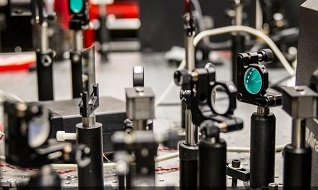
In 2017, University of Utah physicist Valy Vardeny called perovskite a “miracle material” for an emerging field of next-generation electronics, called spintronics, and he’s standing by that assertion. In a paper published today in Nature Communications, Vardeny, along with Jingying Wang, Dali Sun (now at North Carolina State University) and colleagues present two devices built using perovskite to demonstrate the material’s potential in spintronic systems. Its properties, Vardeny says, bring the dream of a spintronic transistor one step closer to reality.
Spintronics
A conventional digital electronic system conveys a binary signal (think 1s and 0s) through pulses of electrons carried through a conductive wire. Spintronics can convey additional information via another characteristic of electrons, their spin direction (think up or down). Spin is related to magnetism. So spintronics uses magnetism to align electrons of a certain spin, or “inject” spin into a system.
If you’ve ever done the old science experiment of turning a nail into a magnet by repeatedly dragging a magnet along its length, then you’ve already dabbled in spintronics. The magnet transfers information to the nail. The trick is then transporting and manipulating that information, which requires devices and materials with finely tuned properties. Researchers are working toward the milestone of a spin transistor, a spintronics version of the electronic components found in practically all modern electronics. Such a device requires a semiconductor material in which a magnetic field can easily manipulate the direction of electrons’ spin—a property called spin-orbit coupling. It’s not easy to build such a transistor, Wang says. “We keep searching for new materials to see if they’re more suitable for this purpose.”
Here’s where perovskites come into play.
Perovskites
Perovskites are a class of mineral with a particular atomic structure. Their value as a technological material has only became apparent in the past 10 years. Because of that atomic structure, researchers have been developing perovskite into a material for making solar panels. By 2018 they’d achieved an efficiency of up to 23 percent of solar energy converted to electrical energy—a big step up from 3.8 percent in 2009.
In the meantime, Vardeny and his colleagues were exploring the possibilities of spintronics and the various materials that could prove effective in transmitting spin. Because of heavy lead atoms in perovskite, physicists predicted that the mineral may possess strong spin-orbit coupling. In a 2017 paper, Vardeny and physics assistant professor Sarah Li showed that a class of perovskites called organic-inorganic hybrid perovskites do indeed possess large spin-orbit coupling. Also, the lifetime of spin injected into the hybrid materials lasted a relatively long time. Both results suggested that this kind of hybrid perovskite held promise as a spintronics material.
Page 1 of 2
Share on:


Suggested Items
IPC APEX EXPO: Some Thoughts About Growth
05/16/2024 | Dan Feinberg, I-Connect007After two and a half days of wandering the aisles at IPC APEX EXPO 2024, for the first time, I almost felt like I was exploring CES. There were so many booths and exhibits that I could describe, but I’d like to focus on the growth and huge value of this event, which has expanded well beyond just the growing and impressive exhibit show floor.
The Shaughnessy Report: Unlock Your High-speed Material Constraints
05/15/2024 | Andy Shaughnessy -- Column: The Shaughnessy ReportThe world of PCB materials used to be a fairly simple one. It was divided into two groups: the “traditional” laminates, often called FR-4, and the high-speed laminates developed especially for high-speed PCBs. These were two worlds that usually didn’t collide. But then traditional laminates started getting better, and high-speed designers and design engineers took notice and started to reconsider what FR-4 could be used for.
Breaking High-speed Material Constraints: Design007 Magazine — May 2024
05/14/2024 | I-Connect007 Editorial TeamDo you need specialty materials for your high-speed designs? Maybe not. Improvements in resins mean designers of high-speed boards can sometimes use traditional laminate systems instead of high-speed materials, saving time and money while streamlining the fab process. In the May 2024 issue of Design007 Magazine, our contributors explain how to avoid overconstraining your materials when working with high-speed boards.
Indium Experts to Present at Electronics in Harsh Environments SMTA Conference
05/13/2024 | Indium Corporationndium Corporation Technical Manager for Europe, Africa, and the Middle East, Karthik Vijay, will deliver a technical presentation and Indium Corporation Senior Technologist, Dr. Ronald Lasky, will deliver both a workshop and technical presentation at the Electronics in Harsh Environments SMTA Conference on May 14-16 in Copenhagen, Denmark.
Ansys’ Collaboration with Schrödinger will Accelerate Materials Development with Unprecedented Multiscale Simulation
05/09/2024 | ANSYSAnsys and Schrödinger are collaborating to deliver an ICME approach that bridges the gap between materials discovery and product development.