


 It’s Only Common Sense: Nice Guys Really Can Finish First
 The Right Approach: I Hear the Train A Comin'
 Marcy's Musings: The Growing Industry
Printing OLED Displays: Has its Time Finally Come?
February 25, 2019 | IDTechExEstimated reading time: 6 minutes
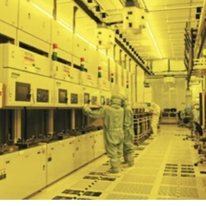
The processing of solution OLED materials over large areas and in a commercial production is not, and has not been, easy. However, as can be seen below, the community now has extensive accumulated knowhow. This is because it has been working on printing OLEDs for over 15 years. Indeed, the first commercial product with a printed OLED display appeared as early as 2004. Granted, this was a small passive matrix display. Since then there have been numerous prototypes. As shown below, these prototypes often targeted large area displays, e.g., TVs, since the benefits of printing are stronger in that size range. Furthermore, large area displays can do with low PPI levels, thus relaxing fine feature printing requirements. Of course, there have also been small-sized high-PPI demonstrators but there are far fewer since the commercial motivation behind them is weaker.
Market Forecast
Today, inkjet printed mid-size, e.g., 21.6", 204PPI OLEDs displays are transitioning into production by a Japanese consortium. This consortium brings together Japanese material suppliers, equipment makers, and display manufacturers. We feel that the objective of the consortium is to pool the early risks involved in the learning curve of printing OLED displays. But once the technical hurdles are sufficiently overcome and the technology is mature enough, there will likely be a tech transfer from the consortium to a display maker.
Interest is not limited to Japanese and Chinese makers though. In fact, even today's leading OLED manufacturers are, and have been, actively developing printing technology. Indeed, there are many strong strategic motivations that keep printing firmly on the agenda. First, those with an FMM technology want to urgently obtain or establish a technology towards large are OLED displays. Second, incumbents are concerned that printing can one day bring about a step change in the production cost, thus reconfiguring the competitiveness map to leave them behind. Third, they see the mastery of display printing as being essential for quantum dot (QD) displays.
In the latter case printing is/will be heavily used. It will be used in QD colour filter displays both on LCDs and OLEDs. More importantly, in the long term, it will be used to develop the ultimate QLED (quantum dot light emitting diode). We say ultimate because this display technology, despite its current immaturity and technology challenges, offers complete contrast, extremely wide colour gamut, thinness, flexibility, etc.
In general, printing can no longer be dismissed as immature or futuristic. Material-side progress has eliminated or substantially narrowed the EQE penalty that traditionally would have to be paid when adopting printed materials. Steady long-term progress on the processing-side is also enabling commercial production.
Of course, there is much further progress to accomplish. The process yield and TACT will need to be further improved. The dimensions of the commercially printed OLEDs displays will need to be enlarged from the monitor to the TV range. The lifetime of solution OLEDs will need to be further extended especially if the end product is to have an extend lifecycle. The printing resolution will need to become finer.
These ongoing development trends are however often incremental in nature and are present in almost all display technologies. The important point is that printed OLEDs have already broken through enough technical barriers to demonstrate their viability. As such, printed OLEDs have becoming an exciting topic. We think this is a space to closely watch in the coming years.
Page 2 of 2Share on:


Suggested Items
IDTechEx Report on Quantum Technology: Nano-scale Physics for Massive Market Impact
04/30/2024 | PRNewswireThe quantum technology market leverages nano-scale physics to create revolutionary new devices for computing, sensing, and communications. Across the industry, quantum technology offers a paradigm shift in performance compared with incumbent solutions.
TSMC Certifies Ansys Multiphysics Platforms, Enabling Next-Gen AI and HPC Chips
04/30/2024 | PRNewswireAnsys announced the certification of its power integrity platforms for TSMC's N2 technology full production release. Both Ansys RedHawk-SC and Ansys Totem are certified for power integrity signoff on the N2 process, delivering significant speed and power advantages for high performance computing, mobile chips, and 3D-IC designs.
Koh Young Extends Invitation to the 2024 IEEE Electronic Components and Technology Conference
04/30/2024 | Koh YoungKoh Young, the industry leader in True3D measurement-based inspection solutions, invites you to join us at the at the 2024 IEEE Electronic Components and Technology Conference from May 28-31, 2024, in Denver, Colorado at the Gaylord Rockies Resort & Convention Center.
Samsung Electronics Begins Industry’s First Mass Production of 9th-Gen V-NAND
04/29/2024 | Samsung ElectronicsSamsung Electronics, the world leader in advanced memory technology, today announced that it has begun mass production for its one-terabit (Tb) triple-level cell (TLC) 9th-generation vertical NAND (V-NAND), solidifying its leadership in the NAND flash market.
TSMC Celebrates 30th North America Technology Symposium
04/29/2024 | TSMCTSMC unveiled its newest semiconductor process, advanced packaging, and 3D IC technologies for powering the next generation of AI innovations with silicon leadership at the Company’s 2024 North America Technology Symposium.