


 Material Insight: The Dielectric Constant of PCB Materials
 American Made Advocacy: What About the Rest of the Technology Stack?
 It’s Only Common Sense: Great Ideas From John Mitchell’s Book on Hiring Habits
When Semiconductors Stick Together, Materials Go Quantum
March 8, 2019 | Lawrence Berkeley National LaboratoryEstimated reading time: 4 minutes
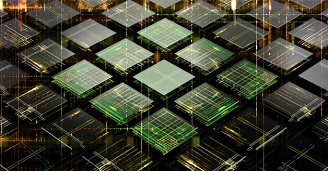
A team of researchers led by the Department of Energy’s Lawrence Berkeley National Laboratory (Berkeley Lab) has developed a simple method that could turn ordinary semiconducting materials into quantum machines—superthin devices marked by extraordinary electronic behavior.
Image Caption: A method developed by a Berkeley Lab-led research team may one day turn ordinary semiconducting materials into quantum electronic devices. (Credit: iStock.com/NiPlot)
Such an advancement could help to revolutionize a number of industries aiming for energy-efficient electronic systems—and provide a platform for exotic new physics.
The study describing the method, which stacks together 2D layers of tungsten disulfide and tungsten diselenide to create an intricately patterned material, or superlattice, was published online recently in the journal Nature.
“This is an amazing discovery because we didn’t think of these semiconducting materials as strongly interacting,” said Feng Wang, a condensed matter physicist with Berkeley Lab’s Materials Sciences Division and professor of physics at UC Berkeley. “Now this work has brought these seemingly ordinary semiconductors into the quantum materials space.”
Image Caption: The twist angle formed between atomically thin layers of tungsten disulfide and tungsten diselenide acts as a “tuning knob,” transforming these semiconductors into an exotic quantum material. (Credit: Berkeley Lab) (Credit: Berkeley Lab)
Two-dimensional (2D) materials, which are just one atom thick, are like nanosized building blocks that can be stacked arbitrarily to form tiny devices. When the lattices of two 2D materials are similar and well-aligned, a repeating pattern called a moiré superlattice can form.
For the past decade, researchers have been studying ways to combine different 2D materials, often starting with graphene—a material known for its ability to efficiently conduct heat and electricity. Out of this body of work, other researchers had discovered that moiré superlattices formed with graphene exhibit exotic physics such as superconductivity when the layers are aligned at just the right angle.
The new study, led by Wang, used 2D samples of semiconducting materials—tungsten disulfide and tungsten diselenide—to show that the twist angle between layers provides a “tuning knob” to turn a 2D semiconducting system into an exotic quantum material with highly interacting electrons.
Page 1 of 2
Share on:


Suggested Items
Material Insight: The Dielectric Constant of PCB Materials
05/17/2024 | Dr. Preeya Kuray -- Column: Material InsightIn the world of PCB design, miniaturization can be achieved by using low dielectric constant (Dk) materials. Low Dk materials can allow for a reduction in thickness while maintaining a given trace width, leading to lower transmission loss and higher density circuitry.
IPC APEX EXPO: Some Thoughts About Growth
05/16/2024 | Dan Feinberg, I-Connect007After two and a half days of wandering the aisles at IPC APEX EXPO 2024, for the first time, I almost felt like I was exploring CES. There were so many booths and exhibits that I could describe, but I’d like to focus on the growth and huge value of this event, which has expanded well beyond just the growing and impressive exhibit show floor.
The Shaughnessy Report: Unlock Your High-speed Material Constraints
05/15/2024 | Andy Shaughnessy -- Column: The Shaughnessy ReportThe world of PCB materials used to be a fairly simple one. It was divided into two groups: the “traditional” laminates, often called FR-4, and the high-speed laminates developed especially for high-speed PCBs. These were two worlds that usually didn’t collide. But then traditional laminates started getting better, and high-speed designers and design engineers took notice and started to reconsider what FR-4 could be used for.
Breaking High-speed Material Constraints: Design007 Magazine — May 2024
05/14/2024 | I-Connect007 Editorial TeamDo you need specialty materials for your high-speed designs? Maybe not. Improvements in resins mean designers of high-speed boards can sometimes use traditional laminate systems instead of high-speed materials, saving time and money while streamlining the fab process. In the May 2024 issue of Design007 Magazine, our contributors explain how to avoid overconstraining your materials when working with high-speed boards.
Indium Experts to Present at Electronics in Harsh Environments SMTA Conference
05/13/2024 | Indium Corporationndium Corporation Technical Manager for Europe, Africa, and the Middle East, Karthik Vijay, will deliver a technical presentation and Indium Corporation Senior Technologist, Dr. Ronald Lasky, will deliver both a workshop and technical presentation at the Electronics in Harsh Environments SMTA Conference on May 14-16 in Copenhagen, Denmark.