


 Material Insight: The Dielectric Constant of PCB Materials
 American Made Advocacy: What About the Rest of the Technology Stack?
 It’s Only Common Sense: Great Ideas From John Mitchell’s Book on Hiring Habits
Scientists 3D-Print All-Liquid ‘Lab on a Chip’
April 29, 2019 | Berkeley LabEstimated reading time: 4 minutes
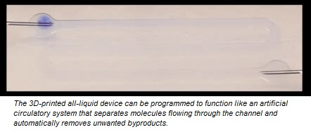
Researchers at DOE’s Lawrence Berkeley National Laboratory (Berkeley Lab) have 3D-printed an all-liquid device that, with the click of a button, can be repeatedly reconfigured on demand to serve a wide range of applications—from making battery materials to screening drug candidates.
“What we demonstrated is remarkable. Our 3D-printed device can be programmed to carry out multistep, complex chemical reactions on demand,” said Brett Helms, a staff scientist in Berkeley Lab’s Materials Sciences Division and Molecular Foundry, who led the study. “What’s even more amazing is that this versatile platform can be reconfigured to efficiently and precisely combine molecules to form very specific products, such as organic battery materials.”
The study’s findings, which were reported in the journal Nature Communications, is the latest in a series of experiments at Berkeley Lab that fabricate all-liquid materials with a 3D printer.
Last year, a study co-authored by Helms and Thomas Russell, a visiting researcher from the University of Massachusetts at Amherst who leads the Adaptive Interfacial Assemblies Toward Structured Liquids Program in Berkeley Lab’s Materials Sciences Division, pioneered a new technique for printing various liquid structures—from droplets to swirling threads of liquid—within another liquid.
Image Caption: When two liquids—one containing nanoscale clay particles, another containing polymer particles—are printed onto a glass substrate, they come together at the interface of the two liquids and within milliseconds form a very thin channel or tube about 1 millimeter in diameter.
“After that successful demonstration, a bunch of us got together to brainstorm on how we could use liquid printing to fabricate a functioning device,” said Helms. “Then it occurred to us: If we can print liquids in defined channels and flow contents through them without destroying them, then we could make useful fluidic devices for a wide range of applications, from new types of miniaturized chemical laboratories to even batteries and electronic devices.”
To make the 3D-printable fluidic device, lead author Wenqian Feng, a postdoctoral researcher in Berkeley Lab’s Materials Sciences Division, designed a specially patterned glass substrate. When two liquids—one containing nanoscale clay particles, another containing polymer particles—are printed onto the substrate, they come together at the interface of the two liquids and within milliseconds form a very thin channel or tube about 1 millimeter in diameter.
Once the channels are formed, catalysts can be placed in different channels of the device. The user can then 3D-print bridges between channels, connecting them so that a chemical flowing through them encounters catalysts in a specific order, setting off a cascade of chemical reactions to make specific chemical compounds. And when controlled by a computer, this complex process can be automated “to execute tasks associated with catalyst placement, build liquid bridges within the device, and run reaction sequences needed to make molecules,” said Russell.
Page 1 of 2
Share on:


Suggested Items
Material Insight: The Dielectric Constant of PCB Materials
05/17/2024 | Dr. Preeya Kuray -- Column: Material InsightIn the world of PCB design, miniaturization can be achieved by using low dielectric constant (Dk) materials. Low Dk materials can allow for a reduction in thickness while maintaining a given trace width, leading to lower transmission loss and higher density circuitry.
IPC APEX EXPO: Some Thoughts About Growth
05/16/2024 | Dan Feinberg, I-Connect007After two and a half days of wandering the aisles at IPC APEX EXPO 2024, for the first time, I almost felt like I was exploring CES. There were so many booths and exhibits that I could describe, but I’d like to focus on the growth and huge value of this event, which has expanded well beyond just the growing and impressive exhibit show floor.
The Shaughnessy Report: Unlock Your High-speed Material Constraints
05/15/2024 | Andy Shaughnessy -- Column: The Shaughnessy ReportThe world of PCB materials used to be a fairly simple one. It was divided into two groups: the “traditional” laminates, often called FR-4, and the high-speed laminates developed especially for high-speed PCBs. These were two worlds that usually didn’t collide. But then traditional laminates started getting better, and high-speed designers and design engineers took notice and started to reconsider what FR-4 could be used for.
Breaking High-speed Material Constraints: Design007 Magazine — May 2024
05/14/2024 | I-Connect007 Editorial TeamDo you need specialty materials for your high-speed designs? Maybe not. Improvements in resins mean designers of high-speed boards can sometimes use traditional laminate systems instead of high-speed materials, saving time and money while streamlining the fab process. In the May 2024 issue of Design007 Magazine, our contributors explain how to avoid overconstraining your materials when working with high-speed boards.
Indium Experts to Present at Electronics in Harsh Environments SMTA Conference
05/13/2024 | Indium Corporationndium Corporation Technical Manager for Europe, Africa, and the Middle East, Karthik Vijay, will deliver a technical presentation and Indium Corporation Senior Technologist, Dr. Ronald Lasky, will deliver both a workshop and technical presentation at the Electronics in Harsh Environments SMTA Conference on May 14-16 in Copenhagen, Denmark.